
Key Findings
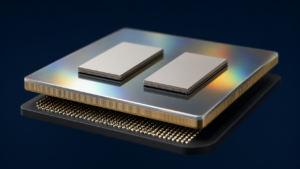
Samsung Electronics is targeting early 2027 for the completion of its 3D Cube-H advanced packaging development. The company plans to release its first design kit by early 2027, which will be followed by evaluations with potential customers. This initiative is part of a broader strategy to strengthen Samsung’s competitiveness in the AI chip manufacturing market and secure orders from major technology firms.
Technical Details
The 3D Cube-H technology transitions from the thermocompression (TC) bonding used in the previous 3D Cube-T to hybrid bonding. This shift enables the vertical stacking of logic chips, increasing transistor density within the same footprint compared to side-by-side arrangements. Key technical specifications include:
- Interconnect Pitch: 3D Cube-H features a pitch of approximately 6 micrometers (μm), a significant reduction from the minimum pitch of around 25μm found in TC bonding-based chips.
- Connection Method: Unlike TC bonding, which uses heat and pressure to join chips via microscopic bumps, hybrid bonding directly connects copper terminals.
- Performance Gains: This direct connection allows for denser interconnections, resulting in improved energy efficiency, performance, and thermal characteristics.
Background and Context
Samsung is expanding its R&D infrastructure to support these advancements. In September, the company opened the Advanced Package Lab (APL) in Yokohama, Japan. Chairman Jay Y. Lee visited the facility on November 1 to review process technologies and materials. Samsung has planned a KRW 350 billion (US$262 million) investment through 2028 to advance packaging R&D and collaborate with Japanese suppliers.
Significance and Outlook
3D Cube-H is intended for high-performance AI applications, specifically the stacking of GPUs or the integration of logic chips with memory devices like HBM. Despite the potential, technical hurdles remain; a Samsung packaging executive noted at ISMP 2026 that preventing void formation and controlling particle contamination are the primary challenges currently facing the development of hybrid bonding.
Get our weekly technology intelligence — free
Receive an infographic that lets you judge at a glance whether each field’s analysis report is worth reading.
Subscribe Free — Weekly Tech Intelligence
By subscribing, you’ll receive Troy-Technical’s weekly technology intelligence newsletter.
- Your email and selected fields are used only to deliver the newsletter.
- We never share your information with third parties.
- You can unsubscribe anytime via the link in each email.
See our Privacy Policy for details.
Takes about a minute · Unsubscribe anytime