Background
The explosive growth of artificial intelligence has driven demand for high-performance High-Bandwidth Memory (HBM) to unprecedented levels. HBM offers superior bandwidth and lower power consumption compared to conventional memory, making it indispensable for the Graphics Processing Units (GPUs) and accelerators powering modern AI data centers. However, HBM manufacturing demands sophisticated stacking techniques and precise packaging, with global capacities for these processes remaining relatively limited. Amidst intensifying technological competition and a desire for enhanced supply chain stability, the U.S. government is aggressively promoting the revitalization of domestic semiconductor manufacturing capabilities, with the CHIPS Act serving as the cornerstone of these initiatives. SK hynix’s latest move is deeply intertwined with these broader international semiconductor strategies.
Key Findings
SK hynix has unveiled plans to invest approximately $4 billion in Indiana, USA, to establish an advanced semiconductor packaging line dedicated to the mass production of High-Bandwidth Memory (HBM). This substantial investment is expected to receive significant support under the U.S. CHIPS Act, with mass production anticipated to commence in late 2028. This represents a strategic initiative to significantly strengthen semiconductor manufacturing capabilities within the United States, thereby driving geographical diversification of the global supply chain while mitigating some of the structural cost challenges historically associated with U.S.-based manufacturing.
Technical Deep Dive
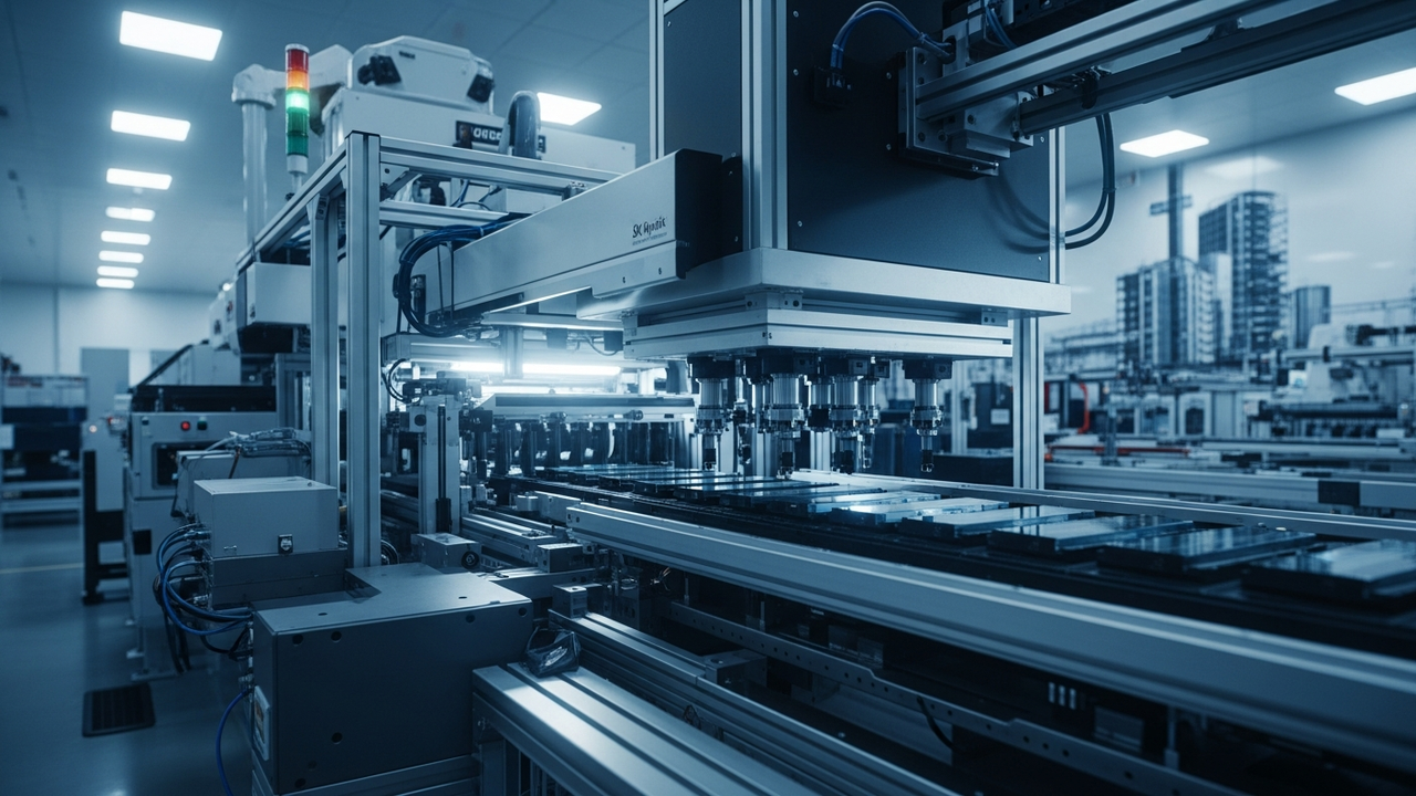
The $4 billion investment will primarily be allocated to building state-of-the-art advanced packaging capabilities for HBM, a critical component for next-generation AI chips. HBM technology is distinguished by its innovative approach of vertically stacking multiple DRAM dies, which dramatically increases memory bandwidth and optimizes connection to processors, thereby maximizing the performance of AI accelerators. Through this facility, SK hynix aims to establish a robust HBM supply capacity within the U.S. market, directly addressing the burgeoning demands of key domestic customers and strengthening regional supply chains for advanced AI hardware.
CHIPS Act and Strategic Rationale
The U.S. CHIPS Act provides substantial subsidies and incentives specifically designed to encourage domestic semiconductor manufacturing and research. SK hynix’s investment is strategically positioned to benefit from this framework, aligning with the CHIPS Act’s objectives to address increasing geopolitical risks and vulnerabilities within global supply chains, ultimately enhancing the economic security and technological sovereignty of the United States. Furthermore, the establishment of an HBM packaging facility in the U.S. signifies a critical geographical diversification of SK hynix’s manufacturing bases. This strategy is designed to distribute manufacturing risks currently concentrated in specific regions and enable the construction of a more resilient global supply chain. From an economic rationality perspective, establishing advanced packaging capabilities in the U.S. is a sound decision, as the cost penalties for back-end operations (packaging) are generally smaller compared to those associated with front-end manufacturing (wafer fabrication).
Market Impact & Outlook
SK hynix’s investment in Indiana is poised to further solidify its leadership in the rapidly expanding HBM market and will significantly contribute to the development of a burgeoning advanced packaging ecosystem within the United States. The planned commencement of mass production in late 2028 strategically aligns with a period when demand for AI infrastructure is projected to intensify even further, suggesting a substantial and timely market impact. For researchers and engineers, this move promises to accelerate R&D and foster talent development in cutting-edge advanced packaging technologies across the U.S. For investors, the combined impact of potential CHIPS Act subsidies and the robust, long-term growth trajectory of HBM demand positions this venture as a key driver for the company’s profitability and stock performance, meriting continued close attention from the financial community.
Source: https://siliconanalysts.com/analysis/micron-samsung-sk-hynix-us-fab-capex-subsidy-war-2
Get our weekly technology intelligence — free
Receive an infographic that lets you judge at a glance whether each field’s analysis report is worth reading.
Subscribe Free — Weekly Tech Intelligence
By subscribing, you’ll receive Troy-Technical’s weekly technology intelligence newsletter.
- Your email and selected fields are used only to deliver the newsletter.
- We never share your information with third parties.
- You can unsubscribe anytime via the link in each email.
See our Privacy Policy for details.
Takes about a minute · Unsubscribe anytime









Comments