Key Findings
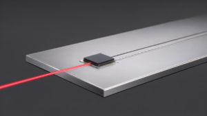
Multiple research teams have presented innovative approaches for on-chip light control and manipulation. Researchers from Seoul National University and the University of Seoul designed a novel photonic integrated circuit on a silicon nitride platform, capable of slowing and delaying light to address the critical need for advanced optical buffers. Concurrently, a collaboration between Harvard SEAS and the Max Planck Institute successfully developed silicon nitride multiplexers (MUXs) that are up to 500 times smaller than conventional layouts, achieved through advanced optimization techniques.
Technical / Clinical Details
The optical buffer developed by the Seoul-based teams leverages the low-loss properties and high refractive index contrast of silicon nitride to temporarily store and precisely release optical signals. This capability is vital for managing traffic and synchronization within data centers and telecommunication networks, ultimately enhancing system efficiency and reliability. The Harvard SEAS and Max Planck multiplexers utilize inverse design, an optimization methodology, to create highly intricate photonic structures. These structures dramatically improve the efficiency of separating and combining optical wavelengths while drastically reducing the physical size of the device. The 500x size reduction compared to traditional MUXs represents a significant advancement towards minimizing footprint and enhancing power efficiency in integrated photonics.
Background & Context
The relentless progression of AI and high-performance computing (HPC) demands ever-increasing data processing speeds and communication bandwidth within data centers. Traditional electronic circuits are facing fundamental limitations in terms of signal delay, power consumption, and footprint, making optical data transmission and processing increasingly indispensable. Optical buffers are essential for sequencing signals and temporary data storage, while multiplexers are critical components for transmitting multiple wavelengths over a single fiber. The miniaturization and performance enhancement of these devices are crucial steps toward realizing next-generation optical interconnects, particularly for co-packaged optics (CPO) and on-chip optical communication.
Strategic Significance & Outlook
These research outcomes are expected to have a profound impact on the fields of optical communication and computing. The optical buffer technology from Seoul National University and the University of Seoul will optimize data center traffic management and improve network responsiveness. Meanwhile, the ultracompact multiplexers from Harvard SEAS and the Max Planck Institute will enable further high-density integration of photonic integrated circuits and more complex on-chip optical functionalities. These advancements will contribute to high-speed data links between AI accelerators, energy-efficient optical interconnects, and the construction of future quantum photonics systems, serving as key enablers for the next frontier of information technology. Silicon nitride, due to its robustness and CMOS compatibility, is projected to remain a central platform for these innovations.
Source: https://www.allaboutcircuits.com/news/three-research-teams-take-different-routes-to-control-light/
Get our weekly technology intelligence — free
Receive an infographic that lets you judge at a glance whether each field’s analysis report is worth reading.
Subscribe Free — Weekly Tech Intelligence
By subscribing, you’ll receive Troy-Technical’s weekly technology intelligence newsletter.
- Your email and selected fields are used only to deliver the newsletter.
- We never share your information with third parties.
- You can unsubscribe anytime via the link in each email.
See our Privacy Policy for details.
Takes about a minute · Unsubscribe anytime