Key Findings
The Japanese consortium Rapidus has unveiled an ambitious advanced packaging roadmap, targeting 600mm panel-level packaging and 8-reticle interposers by 2030 to enable high-density chiplet integration for next-generation AI and high-performance computing (HPC) systems. The company has already commenced validation of 2.xD and 3D packaging processes through the full activation of its Rapidus Chiplet Solutions (RCS) pilot line. This initiative represents a critical technological leap, potentially reshaping the landscape of advanced semiconductor manufacturing and strengthening Japan’s competitive edge in the global supply chain for the AI era.
Technical Details
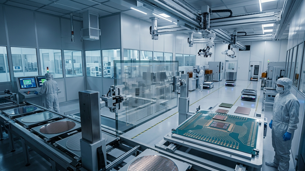
Rapidus’s advanced packaging strategy centers on leveraging larger interposers and pioneering panel-level processing. The interposer roadmap outlines a phased expansion from current 4-reticle (3,320 mm²) designs to 6-reticle (4,980 mm²) by 2028, culminating in 8-reticle (6,640 mm²) by 2030. A cornerstone of this plan is the development of a 600 x 600 mm panel-level packaging platform, which is projected to yield an organic substrate area of approximately 14,400 mm² by 2030. This shift from wafer-based to panel-based processing is expected to deliver significant cost reductions and yield improvements, crucial for high-volume manufacturing. The comprehensive packaging portfolio includes flip-chip BGA, 2.5D silicon interposers, panel-level RDL organic interposers, and advanced 3D stacking techniques via hybrid bonding, all essential for realizing ultra-high-density chiplet integration.
Background and Industry Context
The escalating demands of artificial intelligence and HPC have driven an urgent need for innovations not only in chip fabrication but also in packaging technologies. As the limits of traditional transistor scaling become apparent, heterogeneous integration—the sophisticated method of combining diverse chiplets into a single package—is seen as a key enabler for transcending the limitations of Moore’s Law. Rapidus, with substantial backing from Japan’s Ministry of Economy, Trade and Industry (METI), is concurrently pursuing 2nm process technology development, underscoring its commitment to re-establishing Japan’s prominence in the global semiconductor ecosystem. This dual focus on leading-edge manufacturing and advanced packaging is vital for creating vertically integrated solutions that meet future market demands.
Strategic Significance and Outlook
Rapidus’s aggressive roadmap is a strategic imperative alongside its 2nm process development, forming the core of its integrated semiconductor manufacturing vision. The 600mm panel-level packaging technology, by processing on significantly larger substrates than traditional wafers, promises revolutionary improvements in cost efficiency and throughput. By achieving these targets by 2030, Rapidus aims to establish high-volume production capabilities for next-generation high-performance semiconductors, potentially positioning itself as a key player in the fiercely competitive AI chip market and leading the resurgence of Japan’s semiconductor industry. The move signifies a concerted effort to build a resilient and innovative domestic supply chain.
Get our weekly technology intelligence — free
Receive an infographic that lets you judge at a glance whether each field’s analysis report is worth reading.
Subscribe Free — Weekly Tech Intelligence
By subscribing, you’ll receive Troy-Technical’s weekly technology intelligence newsletter.
- Your email and selected fields are used only to deliver the newsletter.
- We never share your information with third parties.
- You can unsubscribe anytime via the link in each email.
See our Privacy Policy for details.
Takes about a minute · Unsubscribe anytime









Comments