Key Findings
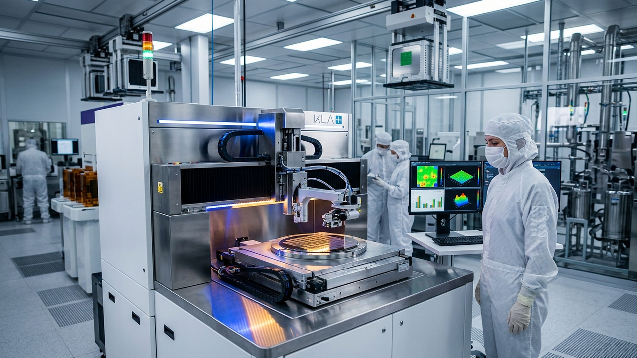
KLA Corporation has announced a new AI (Artificial Intelligence)-algorithm-equipped defect inspection solution that revolutionizes quality control in advanced semiconductor packaging processes. This new equipment is capable of detecting minute defects within high-density RDLs (redistribution layers) and complex 3D stacked structures with greater speed and precision than conventional inspection tools. As AI and HPC (High-Performance Computing) chip performance escalates, advanced packaging technologies like CoWoS (Chip-on-Wafer-on-Substrate) are becoming widespread. However, in these complex structures, subtle defects such as foreign particles, short/open circuits, via failures, and cracks directly impact yield. KLA’s new inspection solution addresses these challenges by identifying and analyzing defects early in the manufacturing process, contributing to overall yield improvement and reduced production costs.
Technical and Solution Details
Key technical features of KLA’s new inspection system include:
- AI-Powered Pattern Recognition: Proprietary AI algorithms automatically learn and differentiate normal from abnormal patterns in vast inspection data. This enables high-precision detection of subtle or new types of defects often missed by traditional rule-based inspections.
- High-Speed Scanning and Data Processing: Advanced optics and image processing technologies allow for rapid, comprehensive scanning of large substrates and wafers. Concurrently, an integrated AI processor provides real-time analysis of detected defect data, supporting swift decision-making.
- 3D Structural Defect Visualization: Combined with 3D imaging techniques like computed tomography (CT), the system visualizes hidden defects within multi-layer structures and bonding imperfections between stacked chips.
- Feedback for Process Control: Detected defect data is fed back into the manufacturing process to optimize parameters and improve engineering, establishing a continuous yield improvement loop.
This solution proves particularly valuable for quality assurance in cutting-edge packaging technologies such as chiplet integration, HBM (High Bandwidth Memory) stacking, and hybrid bonding.
Background and Industry Context
The evolution of advanced packaging technologies has created a new competitive arena within the semiconductor industry, where stabilizing manufacturing yield is paramount. Technologies like CoWoS integrate multiple logic chips and HBM onto a silicon interposer, meaning that interconnect reliability, in addition to component quality, dictates overall yield. As a global leader in semiconductor inspection and metrology, KLA consistently provides solutions for the most advanced challenges. This announcement represents a move to redefine quality control in the era of AI chips.
Strategic Significance and Outlook
KLA plans to further evolve its AI-integrated inspection and metrology solutions to address increasingly complex advanced packaging challenges. Future goals include real-time inline quality control, predictive analytics, and fully automated inspection flows. This will enable semiconductor manufacturers to reduce AI/HPC chip production costs, shorten time-to-market, and strengthen the foundation for accelerating innovation in the AI era.
Source: #
Get our weekly technology intelligence — free
Receive an infographic that lets you judge at a glance whether each field’s analysis report is worth reading.
Subscribe Free — Weekly Tech Intelligence
By subscribing, you’ll receive Troy-Technical’s weekly technology intelligence newsletter.
- Your email and selected fields are used only to deliver the newsletter.
- We never share your information with third parties.
- You can unsubscribe anytime via the link in each email.
See our Privacy Policy for details.
Takes about a minute · Unsubscribe anytime









Comments