

Key Findings
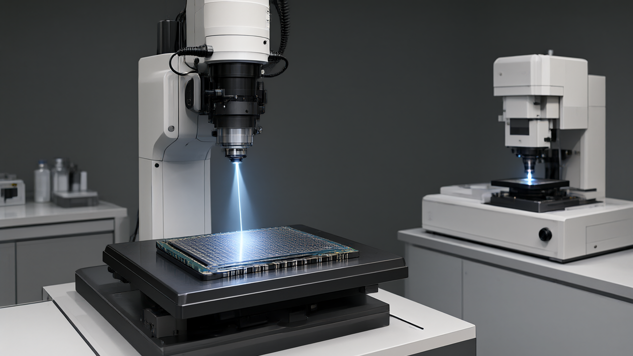
ZEISS SMT is expanding its portfolio to support next-generation semiconductor manufacturing, focusing on advanced packaging and critical lithography processes. The company has introduced the ZEISS NLX and ZEISS DUNE systems to manage the increased complexity of chip architectures, specifically where multiple chips or chiplets are integrated into compact spaces.
Technical Details: Advanced Packaging
- ZEISS NLX: A non-destructive inspection system designed for 300-millimeter wafers. It allows manufacturers to visualize internal structures in chip packages, such as connections between stacked dies, to detect defects early. It is compatible with both process development and high-volume production.
- ZEISS DUNE: A metrology system that measures and individually corrects wafer bow. By managing wafer topography, the system helps avoid yield losses in downstream processing and prepares wafers for bonding processes.
Technical Details: Lithography and Photomasks
To ensure stable lithography, ZEISS SMT provides specialized photomask solutions. The ZEISS AIMS EUV 3.0 inspects photomasks under optical conditions that mirror those of the wafer scanner, allowing for the detection of critical defects before production. This system supports both Low-NA-EUV and High-NA-EUV lithography and triples mask throughput.
Complementing this is the ZEISS MeRiT system, which enables the targeted repair of the smallest defects on photomasks, providing a final qualification step following the AIMS EUV process.
Significance and Outlook
According to Christoph Hensche, President of ZEISS Semiconductor Manufacturing Optics, the next generation of manufacturing relies on the precise interaction of complex process steps rather than isolated technology leaps. Axel Christian, President of ZEISS North America, emphasizes that as manufacturing becomes more demanding, photomask quality becomes increasingly critical. By combining optical systems, process control, and advanced packaging solutions, ZEISS SMT intends to help customers bring future chip generations into production reliably and productively.
Get our weekly technology intelligence — free
Receive an infographic that lets you judge at a glance whether each field’s analysis report is worth reading.
Subscribe Free — Weekly Tech Intelligence
By subscribing, you’ll receive Troy-Technical’s weekly technology intelligence newsletter.
- Your email and selected fields are used only to deliver the newsletter.
- We never share your information with third parties.
- You can unsubscribe anytime via the link in each email.
See our Privacy Policy for details.
Takes about a minute · Unsubscribe anytime