


Key Findings
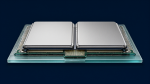
Intel is advancing its multi-chiplet strategy by evolving Embedded Multi-die Interconnect Bridge (EMIB) and Foveros technologies to create larger, more efficient system-in-packages (SiPs). The company’s ultimate objective is to build SiPs the size of 12 reticles using EMIB and Foveros Direct 3D. This transition allows Intel to deliver performance enhancements cost-efficiently while scaling chips in every direction.
Technical Details of EMIB Evolution
EMIB has transitioned from a simple alternative to silicon interposers to a sophisticated system for high-density die-to-die connectivity. Key technical milestones include:
- Bump Pitch Reduction: First-layer-interconnect (FLI) bump pitch has decreased from 55 µm to 45 µm, with future targets of 36 µm and eventually 25 µm to increase shoreline density.
- EMIB-M: Incorporates metal-insulator-metal (MIM) capacitors to improve power delivery and suppress voltage fluctuations.
- EMIB-T: Adds through-silicon vias (TSVs) to enable vertical power travel, reducing impedance and noise. This is critical for multi-kilowatt SiPs and HBM4-class memory.
- Physical Scaling: Package sizes have grown from 4X reticle (80×80 mm) to 8X reticles (120×120 mm), with future 12X SiPs planned for 120×180 mm packages.
Background and Context
Intel began its advanced packaging journey in 2017 with Stratix 10 FPGAs and Kaby Lake-G CPUs. Following challenges with initial 10nm process technology, the company shifted toward a multi-chiplet strategy. Today, EMIB and Foveros are no longer separate technologies but complementary building blocks used across most of Intel’s recent client and data center CPU products, including Xeon 6 ‘Granite Rapids’.
Significance and Outlook
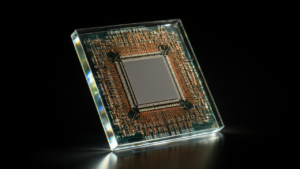
The integration of glass-core substrates is expected to be a major advancement for EMIB, providing better stability and reduced warpage for enormous packages. Intel states that EMIB-T is on track for mass production in 2027, with yields and reliability meeting targets. According to CEO Lip Bu Tan, the technology is essential for advanced AI silicon solutions that are not possible with current mainstream offerings.
Get our weekly technology intelligence — free
Receive an infographic that lets you judge at a glance whether each field’s analysis report is worth reading.
Subscribe Free — Weekly Tech Intelligence
By subscribing, you’ll receive Troy-Technical’s weekly technology intelligence newsletter.
- Your email and selected fields are used only to deliver the newsletter.
- We never share your information with third parties.
- You can unsubscribe anytime via the link in each email.
See our Privacy Policy for details.
Takes about a minute · Unsubscribe anytime