

Key Findings
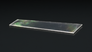
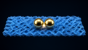
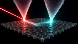
Professor Woo-Hee Kim and colleagues have introduced a method called etching-flux-mediated single-centred nucleation (EF-SCN) that allows for the precise placement and growth of two-dimensional (2D) semiconductor crystals. Using this technique, the team produced molybdenum disulfide (MoS2) crystals approximately 8 micrometers across and single-crystal films that filled 10-micrometre growth regions. On a 2-centimetre substrate, the process demonstrated a single-crystal yield of over 99%.
Technical Details
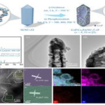
The EF-SCN process utilizes metal-organic chemical vapor deposition on patterned substrates. The researchers surrounded growth regions with an oxide barrier—specifically hafnium oxide (HfO2)—which releases oxygen when heated to 750°C. This oxygen etches material near the pattern boundaries, suppressing nucleation at the edges and forcing a single crystal to form at the center, which then expands outwards.
- Temperature Optimization: By replacing HfO2 with zirconium dioxide, the team reduced the required crystallization temperature, enabling the growth of triangular single-crystal MoS2 domains at temperatures as low as 430°C.
- Growth Control: The flow rate of diethyl sulfide regulates the number of nuclei, while the molybdenum precursor flow rate determines the extent of crystal growth.
- Device Performance: Field-effect transistors fabricated via EF-SCN achieved a field-effect mobility of up to 117 cm2 V-1s-1. Four transistors integrated within a single crystal showed only 7.8% variation in electron mobility.
Background & Context
In semiconductor manufacturing, nucleation determines where and how crystals grow. Conventional area-selective growth methods often fail to reliably control nucleation within designated regions, hindering the production of large single crystals and precisely aligned structures necessary for next-generation electronic devices.
Significance & Outlook
The EF-SCN method provides a general framework for programming nucleation position and crystal geometry. By enabling highly reproducible single-crystal growth and the creation of line-shaped channels for transistor integration, this approach facilitates the construction of denser electronic circuits with more consistent performance.
Source: https://www.miragenews.com/hanyang-researchers-control-where-semiconductor-1773269/
Get our weekly technology intelligence — free
Receive an infographic that lets you judge at a glance whether each field’s analysis report is worth reading.
Subscribe Free — Weekly Tech Intelligence
By subscribing, you’ll receive Troy-Technical’s weekly technology intelligence newsletter.
- Your email and selected fields are used only to deliver the newsletter.
- We never share your information with third parties.
- You can unsubscribe anytime via the link in each email.
See our Privacy Policy for details.
Takes about a minute · Unsubscribe anytime