

Key Findings
Hummink has introduced the BIRD module, a system designed to integrate micron-scale printing and defect repair directly into manufacturing processes. The module utilizes Hummink’s proprietary High Precision Capillary Printing (HPCaP) technology to perform localized material deposition and surface functionalization. The system is currently deployed in a pilot line at a major semiconductor and display manufacturer in Asia.
Technical Details
The BIRD module employs a direct additive process consisting of maskless deposition followed by local laser sintering, allowing the cycle from design to finished part to be completed in a few minutes. Technical specifications include:
- Printing resolution: 0.6 to 50 µm.
- Ink compatibility: Conductive, dielectric, and functional inks with viscosities up to 250,000 cP.
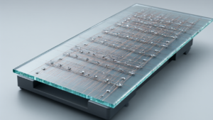
- Substrate compatibility: Glass and a wide range of other substrates.
Background and Context
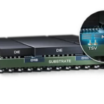
The technology addresses critical yield challenges in advanced packaging, particularly as the industry shifts toward Fan-Out Panel-Level Packaging (FOPLP). In these environments, complex architectures and finer Redistribution Layer (RDL) lines increase the risk of defects. Because a single RDL defect can result in the scrapping of an entire panel, the ability to repair rather than discard substrates can recover value reaching tens of thousands of euros per substrate.
Significance and Outlook
While HPCaP technology has been demonstrated in R&D environments, the BIRD module represents its transition into production environments. By reducing material and chemical consumption through targeted deposition, the module aims to minimize scrap rates. This capability is particularly relevant for manufacturers operating in the AI, multi-chip architecture, and information and communications technology (ICT) sectors. Following its current pilot phase in display manufacturing, Hummink intends to apply the technology to semiconductor manufacturing and advanced packaging.
Source: https://www.semiconductor-digest.com/hummink-unveils-the-bird-module-at-semicon-europa-2026/
Get our weekly technology intelligence — free
Receive an infographic that lets you judge at a glance whether each field’s analysis report is worth reading.
Subscribe Free — Weekly Tech Intelligence
By subscribing, you’ll receive Troy-Technical’s weekly technology intelligence newsletter.
- Your email and selected fields are used only to deliver the newsletter.
- We never share your information with third parties.
- You can unsubscribe anytime via the link in each email.
See our Privacy Policy for details.
Takes about a minute · Unsubscribe anytime