New Technology– category –
-

TRUMPF Resolves Glass Substrate TGV Coating Bottleneck with High-Power HiPIMS, Accelerating Next-Gen AI Chip Packaging Mass Production
Asianews.network Germany Overview Germany's TRUMPF announced a breakthrough in Through Glass Via (TGV) coating for glass substrates, a critical bottleneck, by leveraging its high-power HiPIMS (High Power Impulse Magnetron Sputtering) tec... -
Samsung Dedicates Half of Its 4nm Foundry Capacity to HBM4 Base Dies Amid AI Boom
ZDNet Korea South Korea Overview Samsung Electronics is reportedly allocating over 50% of its advanced 4nm foundry capacity—specifically 15,000 wafers per month out of an estimated 30,000 total—to the production of HBM4 base dies. This s... -
Samsung Electro-Mechanics Unveils Five Next-Gen Semiconductor Package Substrate Products for AI, Automotive, and Mobile Markets at KPCA Show
Global Sources South Korea Overview Samsung Electro-Mechanics showcased next-generation semiconductor package substrate technologies at KPCA Show, targeting high-end chip applications like AI servers, automotive systems, and mobile devic... -
Broadcom CEO Warns of Critical Substrate Bottleneck for AI Chips; Toppan Subsidiary Builds Advanced FC-BGA Plant in Singapore
Industry Media Global Overview Broadcom CEO Hock Tan has identified advanced packaging substrates as a critical new bottleneck for high-end chip production, particularly for demanding AI accelerators and network processors, alongside adv... -
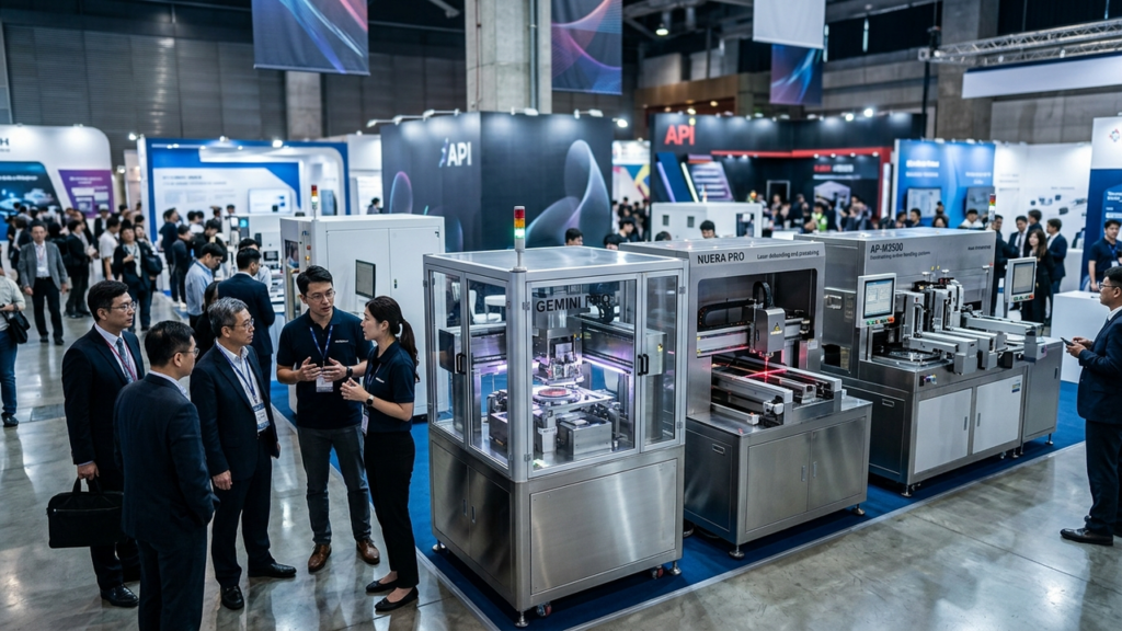
API Unveils GEMINI PRO, NUERA PRO, and AP-M3500 Bonding Platforms for Next-Gen Semiconductors at SEMICON Taiwan 2026, Addressing Key Packaging Bottlenecks
API (Advanced Packaging Intelligence) Unknown Overview API (Advanced Packaging Intelligence) reported a successful exhibition of next-generation advanced packaging technologies at SEMICON Taiwan 2026. Their GEMINI PRO, NUERA PRO, and AP-... -
Samsung Unveils 3D-Stacked Memory Strategy, Featuring HBM5, zHBM, and zNAND-O, to Break AI’s Memory Wall
Design And Reuse South Korea Overview At SEMICON Taiwan 2026, Samsung Electronics presented a bold 3D-stacked memory strategy designed to overcome the limitations of current memory architectures in the AI era. This roadmap introduces HBM... -
Taiwan’s MOEA Unveils 29 Cutting-Edge Semiconductor Innovations, Including Double-Sided RDL Process for CoPoS Packaging at SEMICON Taiwan 2026
Ministry of Economic Affairs (MOEA) Taiwan Overview Taiwan's Ministry of Economic Affairs (MOEA) showcased 29 cutting-edge technology innovations at SEMICON Taiwan 2026, encompassing advanced packaging, AI data center power management, a... -
Samsung Electronics Establishes Advanced Packaging R&D Center in Yokohama to Deepen Collaboration with Japanese Suppliers for HBM Technologies
digitimes South Korea Overview Samsung Electronics has opened an advanced packaging research center in Yokohama, Japan, to strengthen development cooperation with Japanese suppliers of critical materials and equipment for HBM. This strat... -
Samsung Foundry Unveils Next-Gen HBM Architecture Leveraging Advanced Packaging for AI/HPC Performance
Samsung Foundry South Korea Overview Samsung Foundry announced a new HBM architecture that combines advanced logic nodes with advanced packaging, promising significantly higher bandwidth and energy efficiency for AI and HPC systems. Its ... -
Eli Lilly’s Oral GLP-1 Agonist Orforglipron Shows Promising Weight Loss and Safety in Phase 2 Trials, Rivaling Injectables
Endocrinology Today USA Overview Eli Lilly's investigational oral GLP-1 receptor agonist, Orforglipron, demonstrated weight loss comparable to some injectable GLP-1s in Phase 2 trials for obesity and type 2 diabetes. As a non-peptide sma...