Semiconductor Back-End– category –
-

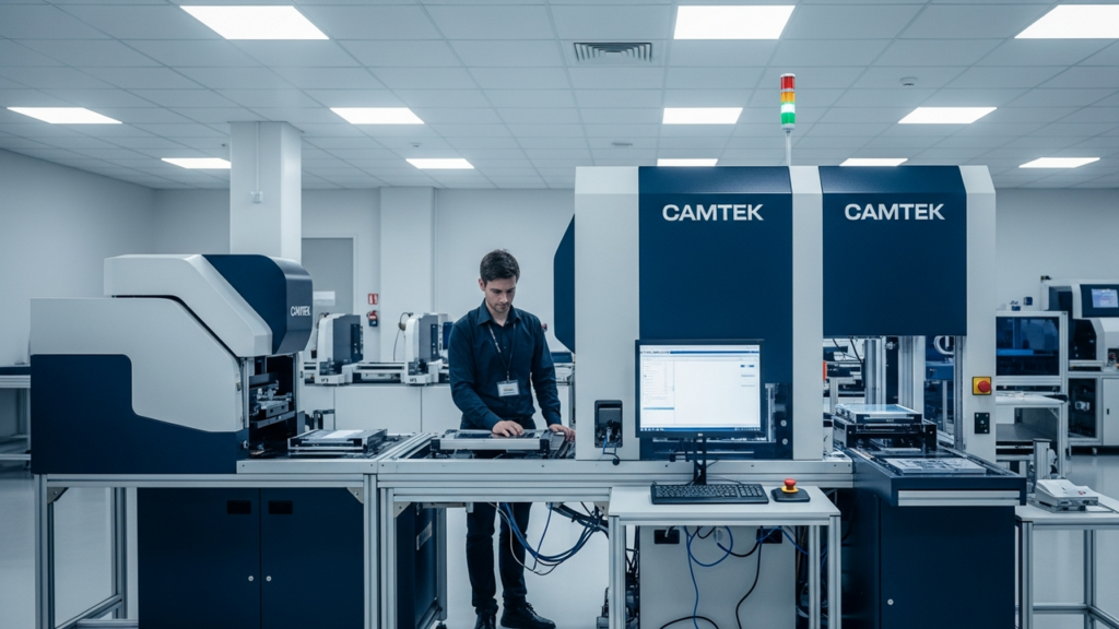
Camtek’s Precision Inspection and Metrology Solutions Drive Yield and Efficiency in Advanced Packaging
Camtek イスラエル Overview Camtek provides industry-leading 2D and 3D inspection and metrology platforms that address the escalating complexity and rapid growth of the advanced packaging market. Featuring sub-micron defect detection, CAD... -
Rapidus Explores Panel-Level Packaging on Glass Substrates for Next-Gen AI/HPC Processors
Tom's Hardware Japan Overview Japanese semiconductor firm Rapidus is actively exploring the adoption of panel-level packaging (PLP) on large 600mm x 600mm glass panels for manufacturing high-end multi-chiplet processors designed for AI a... -
KLA Enhances AI Chip Production with Comprehensive Wafer Inspection and Metrology for Advanced Packaging
KLA USA Overview KLA offers comprehensive inspection and metrology solutions for complex advanced wafer-level packaging processes, including 2.5D/3D integration, WLCSP, and FOWLP. Its AI-powered systems improve yield, defect detection, a... -
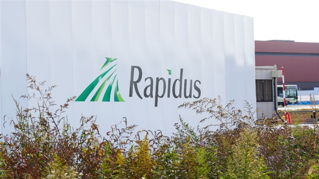
Rapidus to Launch Advanced Packaging Pilot Line in Hokkaido by Spring 2026, Accelerating AI Chip Development
Sic-chip.com (via Digitimes) Japan Overview Japanese semiconductor manufacturer Rapidus is accelerating the development of advanced packaging solutions for AI chips, with plans to commence pilot production at its advanced packaging line ... -
Japan’s Rapidus and LSTC Launch Optoelectronic Advanced Packaging Project to Cut AI Chip Power Consumption
creating nano technologies inc. (via Digitimes) Japan Overview Japan's next-generation semiconductor manufacturer Rapidus, in collaboration with the Leading-edge Semiconductor Technology Center (LSTC) and other institutions, has initiate... -
ASE Technology Boosts Advanced Packaging Investment to Record $8.5 Billion Amid Surging AI Demand
digitimes Taiwan Overview ASE Technology Holding, the world's largest chip packaging and test company, has significantly raised its 2026 capital expenditure to a record $8.5 billion, driven by surging demand for AI chips. The company pro... -
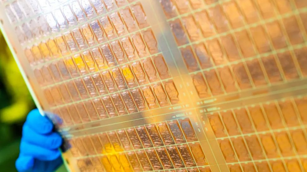
Glass Substrates Emerge as Next-Generation Solution to AI Chip Packaging Bottleneck
TrendForce Taiwan Overview Glass substrates are gaining significant traction as a next-generation material poised to overcome the limitations of traditional organic substrates and resolve critical bottlenecks in AI chip packaging. Offeri... -
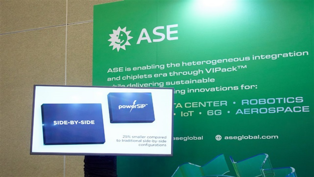
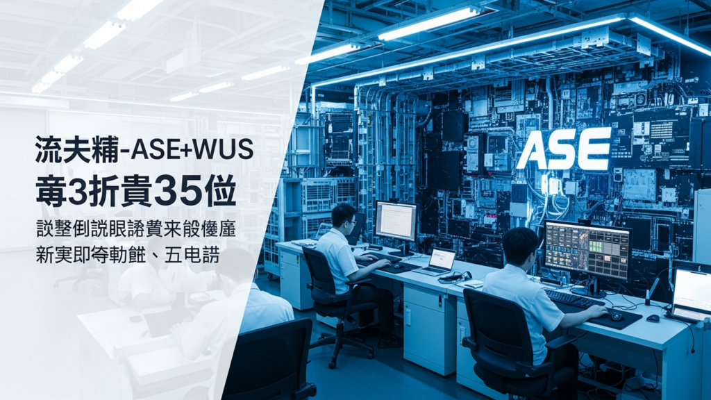
ASE and WUS Announce Strategic Alliance for Advanced AI Packaging Hub in Kaohsiung with NT$35 Billion Investment
ASE Technology Holding Co., Ltd. Taiwan Overview ASE Technology Holding and WUS Printed Circuit have unveiled a strategic collaboration to construct a state-of-the-art manufacturing facility in Kaohsiung, Taiwan, backed by an investment ... -
TSMC Accelerates CoWoS and SoIC Expansion to Quell AI Chip Bottleneck, Targets 4x Capacity by 2026
FinancialContent - Stock Market Taiwan Overview TSMC is aggressively expanding its CoWoS and SoIC advanced packaging capacity to address the soaring demand for AI chips, aiming to increase monthly wafer output from approximately 35,000 u... -
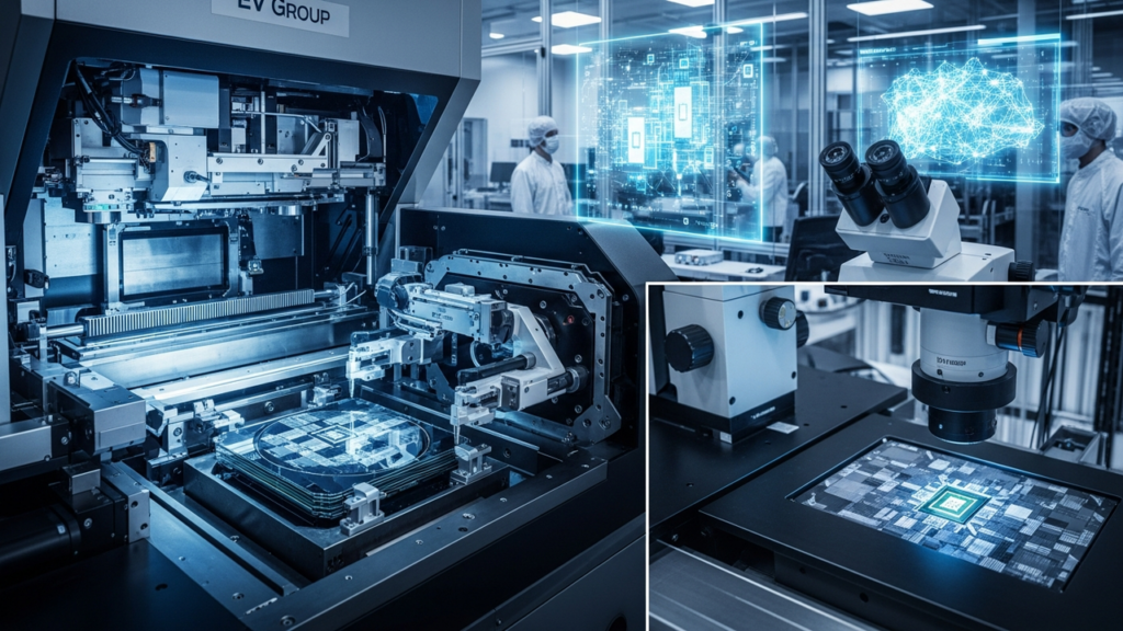
EV Group Unlocks Next-Gen Semiconductor Performance with Advanced Integration Technologies at ECTC 2026
EV Group オーストリア Overview At ECTC 2026, EV Group showcased its latest advancements in hybrid bonding, layer transfer, and maskless lithography, offering crucial solutions for next-generation heterogeneous integration and advanced pa...