Semiconductor Back-End– category –
-

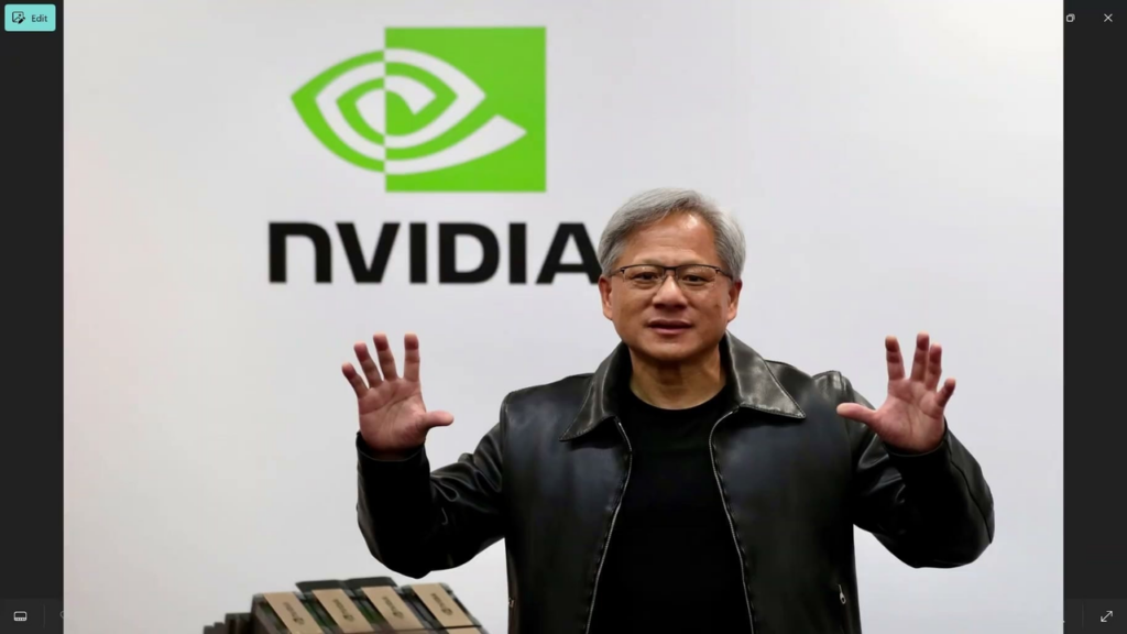
NVIDIA’s CoWoS Bottleneck Eases, HBM Supply Emerges as Primary Constraint for AI Accelerators
24/7 Wall St. USA Overview TSMC's CoWoS advanced packaging capacity for AI accelerators is expanding, projected to reach 35,000 wafers/month by late 2026 and up to 140,000 wafers/month by 2027, alleviating a long-standing bottleneck. How... -
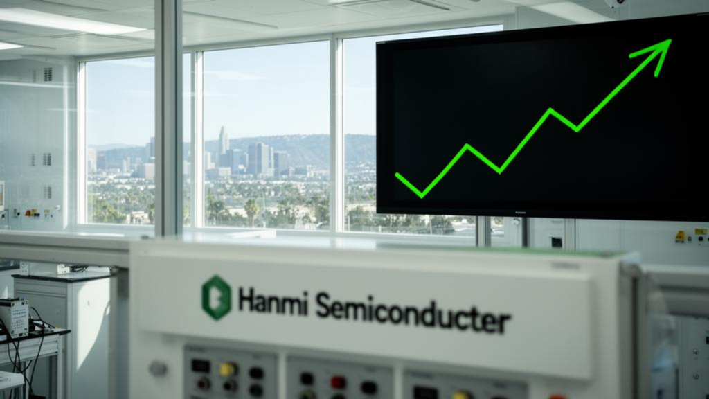
Hanmi Semiconductor Forecasts HBM4 TC Bonder Rebound in Q2, Announces US Expansion Plans
BigGo Finance South Korea Overview Hanmi Semiconductor anticipates a significant rebound in HBM4 TC bonder orders from Q2 2026, driven by accelerating AI semiconductor demand, despite a Q1 slump during the HBM3E-to-HBM4 transition. The c... -
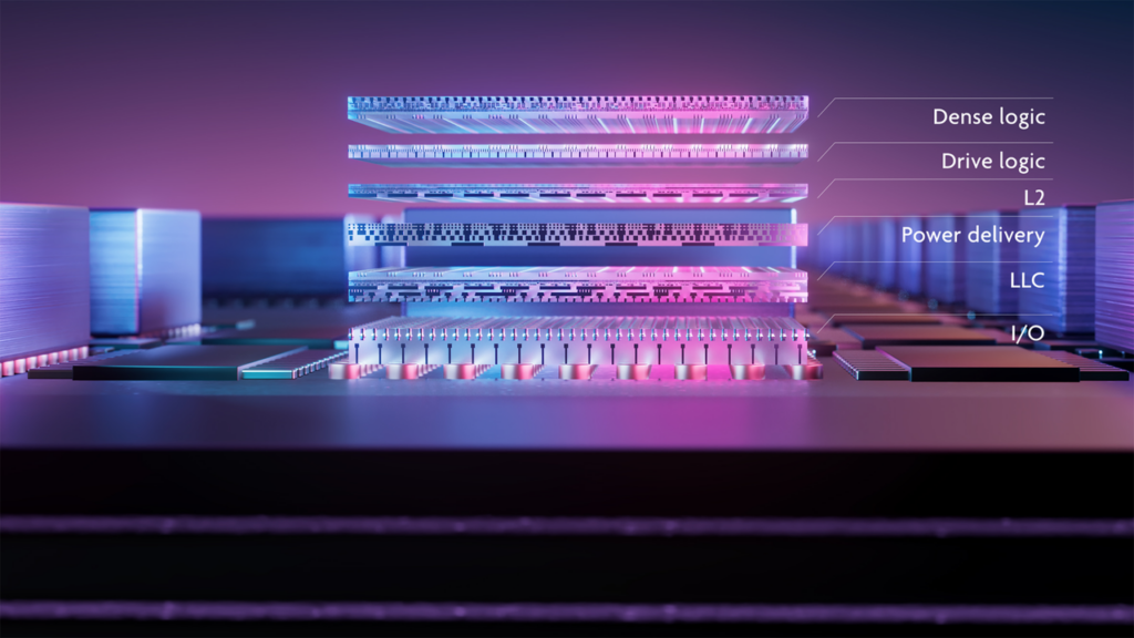
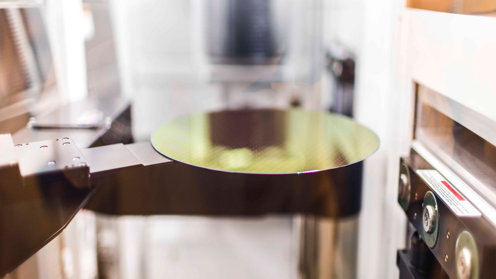
Pushing the Limits of 3D Integration: Imec and EVG Achieve Record 200nm Hybrid Bonding Pitch
imec ベルギー Overview Imec and EV Group (EVG) have announced a major breakthrough in 3D integration, demonstrating wafer-to-wafer hybrid bonding with an unprecedented 200nm copper interconnect pad pitch on 300mm wafers. Achieved with a ... -
ASE Unveils Industry-First Automated 310mm Panel-Level Packaging Line for AI and Chiplet Integration
AnySilicon Taiwan Overview Advanced Semiconductor Engineering (ASE) has developed an automated 310mm x 310mm panel-level packaging (PLP) production line, a significant advancement for AI processors and chiplet architectures. This industr... -
Malaysia Launches National Consortium to Accelerate Advanced Semiconductor Packaging Development Within Two Years
SME.asia Malaysia Overview Malaysia has established the Malaysia Advanced Packaging Consortium (MAPC) with a total funding of RM185 million ($39 million USD) to develop domestic advanced semiconductor packaging capabilities within two ye... -
SK Hynix and Samsung Unveil Production-Ready HBM4 with Hybrid Bonding, Targeting H2 2026 Mass Production
Techfund South Korea Overview At CES 2026, SK Hynix showcased a 16-layer, 48GB HBM4 device leveraging advanced Through-Silicon Via (TSV) and hybrid bonding for high density, while Samsung presented a 12-layer, 36GB HBM4 stack focused on ... -
AMD Commits Over $10 Billion to Taiwan’s AI Ecosystem for Advanced Packaging and EFB Technology Expansion
EE Times Taiwan Overview AMD announced an investment exceeding $10 billion into Taiwan's AI ecosystem, bolstering advanced packaging capabilities and R&D. This initiative specifically targets Elevated Fanout Bridge (EFB) based 2.5D p... -
TSMC Repurposes Mature Node Capacity to CoWoS for AI Accelerators Amid Critical Supply Shortage
Tom's Hardware Taiwan Overview TSMC is reallocating 40-90nm mature node capacity to expand its CoWoS advanced packaging and silicon interposer fabrication, directly addressing a critical supply bottleneck for AI accelerators. This strate... -
Amkor Technology Targets $11B Revenue by 2030, Anchored by $7 Billion Arizona Advanced Packaging Investment
MarketBeat USA Overview Amkor Technology aims to exceed $11 billion in revenue by 2030, driven by a $7 billion, two-phase investment in its Arizona advanced packaging and test campus. High-volume manufacturing is slated to begin in 2028,... -
Semiconductor Back-End Weekly Report May 24, 2026
🎙 Podcast May 24, 2026 (MP3) — Play & Download Semiconductor_BackEndEnglishPodcast_20260524.mp3Download