NVIDIA– tag –
-

HBM Supply Crunch Deepens: DRAM Wafer Production and Advanced Packaging/Test Emerge as Dual Bottlenecks Amid Samsung, SK Hynix, Micron Rivalry
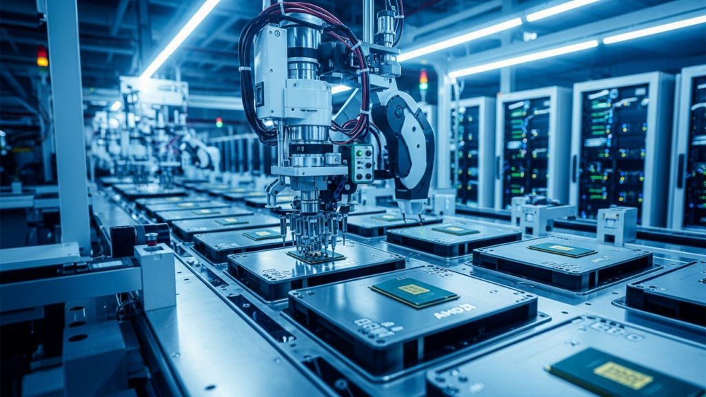
Industry Analysis International Overview High Bandwidth Memory (HBM), central to AI, faces dual bottlenecks in both DRAM wafer manufacturing and advanced packaging/test capacity. HBM achieves high bandwidth and energy efficiency through ... -
TSMC Plans Three Advanced Packaging Plants at Chiayi Science Park, Targeting Mass Production by 2027 for AI and Quantum Tech
Taiwan News Taiwan Overview TSMC plans three advanced packaging plants at Taiwan's Chiayi Science Park, with two slated for mass production by 2027. These facilities will focus on AI, heterogeneous integration, and quantum technology, le... -
Morgan Stanley Forecasts 93% CoWoS Demand Surge by 2027, Driven by AMD’s Venice CPU Shipments
KuCoin International Overview Morgan Stanley forecasts global CoWoS (Chip-on-Wafer-on-Substrate) demand to nearly double to 2.694 million wafers in 2027, a 93% increase from 1.394 million in 2026. This growth is predominantly driven by A... -
Samsung Develops ‘2.xD’ Advanced Packaging Integrating HBM, Logic, and SiPh to Tackle AI Data Center Power and Data Bottlenecks
DigiTimes Taiwan Overview Samsung Electronics is developing '2.xD' advanced packaging technology that integrates HBM, logic chips, and silicon photonics (SiPh) into a single package. This innovation aims to resolve critical power consump... -
Global ABF Substrate Shortage to Persist Through 2028 Due to Soaring AI Demand, Impacting High-End Chip Production
DigiTimes Taiwan Overview The global market for ABF (Ajinomoto Build-up Film) substrates is projected to remain in shortage through 2028, driven by escalating demand for AI hardware. This scarcity directly impacts the production of high-... -
ASE Initiates Largest-Ever Global Expansion to Double CoWoS Capacity to 45,000 Wafers/Month by Late 2027
Industry Blog/Analysis International Overview ASE is undertaking its largest global factory expansion in history, commencing construction of six new packaging and testing plants in 2026. This aggressive ramp aims to increase monthly CoWo... -
Advanced Packaging Becomes the New Bottleneck for AI Chip Production, Driving Global Capex Race and Nvidia’s Supply Diversification Efforts
The Economy International Overview Advanced packaging, not process technology, is now the primary bottleneck in AI chip production, prompting Nvidia to explore diversifying its CoWoS supply, potentially including Intel's EMIB. This shift... -
Lightmatter Joins NVIDIA NVLink Fusion Ecosystem, Boosts AI Data Center Optical Connectivity 8x with First 16-Wavelength Bidirectional DWDM Link
Lightmatter (Official Website) USA Overview Photonic computing company Lightmatter has advanced its photonic computing and interconnect technology for AI data centers, joining the NVIDIA NVLink Fusion ecosystem. The company achieved the ... -
Marvell Technology Accelerates Co-Packaged Optics (CPO) Deployment to Revolutionize AI Scaling
Marvell Technology (YouTube) USA Overview Marvell Technology is accelerating the deployment of Co-Packaged Optics (CPO) as the next leap in AI infrastructure scaling. CPO revolutionizes data center connectivity by directly integrating co... -
MIT’s Electronic-Photonic Chip Achieves Over 1 Pbps Data Transfer, Targets 10 Pbps by 2030 to Resolve AI Energy Crisis
MarketWise USA Overview A novel optical coupler developed through MIT's FUTUR-IC program enables AI chips to transfer data at over 1 petabit per second (Pbps), with ambitions for 10 Pbps by 2030. This electronic-photonic integration dram...