Redistribution Layer– tag –
-

Taiyo Holdings and imec Unveil 700nm 3-Layer RDL Breakthrough for Next-Gen AI Packaging
Quantum Zeitgeist Japan, Belgium Overview Taiyo Holdings, in collaboration with imec, announced at IEEE ESTC 2026 the successful formation of a 3-layer Redistribution Layer (RDL) with a critical dimension of 700 nanometers on 12-inch waf... -
Powertech Technology and Broadcom Establish $400 Million Singapore FOPLP Joint Venture for AI ASICs Manufacturing
DigiTimes Taiwan Overview Powertech Technology (PTI) has approved a $400 million investment in a joint venture with Broadcom in Singapore to build Fan-Out Panel-Level Packaging (FOPLP) manufacturing capacity. This strategic move aims to ... -
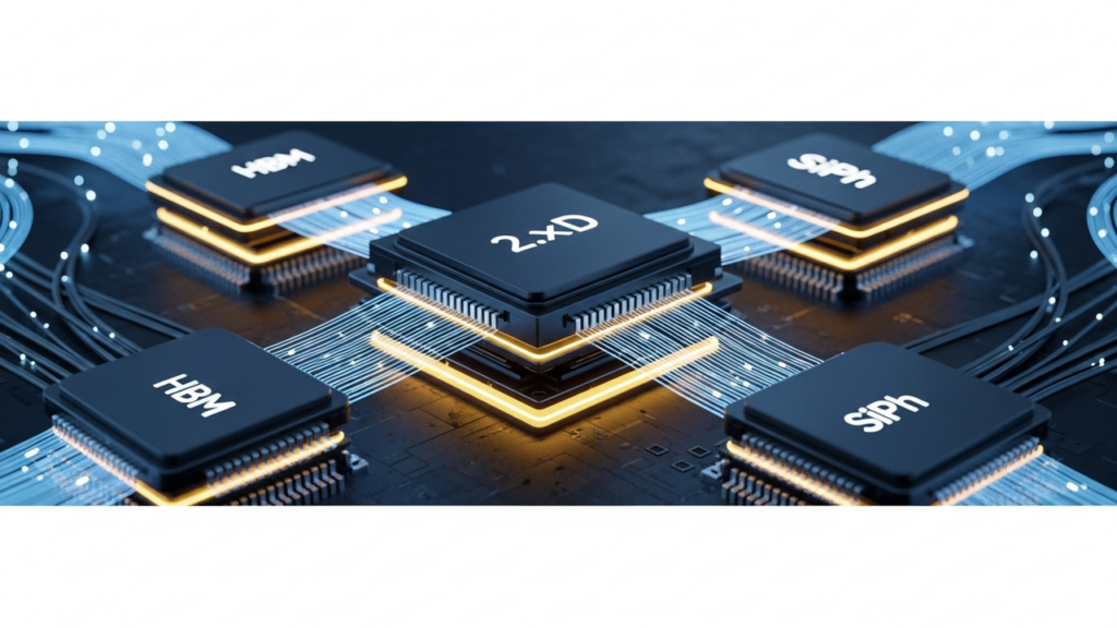
Samsung Electronics Advances “2.xD” Packaging Integrating HBM, Logic, and Optical Tech to Resolve AI Power and Heat Bottlenecks
BigGo Finance South Korea Overview Samsung Electronics is developing "2.xD" next-generation packaging technology that integrates High Bandwidth Memory (HBM), logic chips, and silicon photonics (SiPh) into a single package to address crit... -
Samsung Develops ‘2.xD’ Advanced Packaging Integrating HBM, Logic, and SiPh to Tackle AI Data Center Power and Data Bottlenecks
DigiTimes Taiwan Overview Samsung Electronics is developing '2.xD' advanced packaging technology that integrates HBM, logic chips, and silicon photonics (SiPh) into a single package. This innovation aims to resolve critical power consump... -
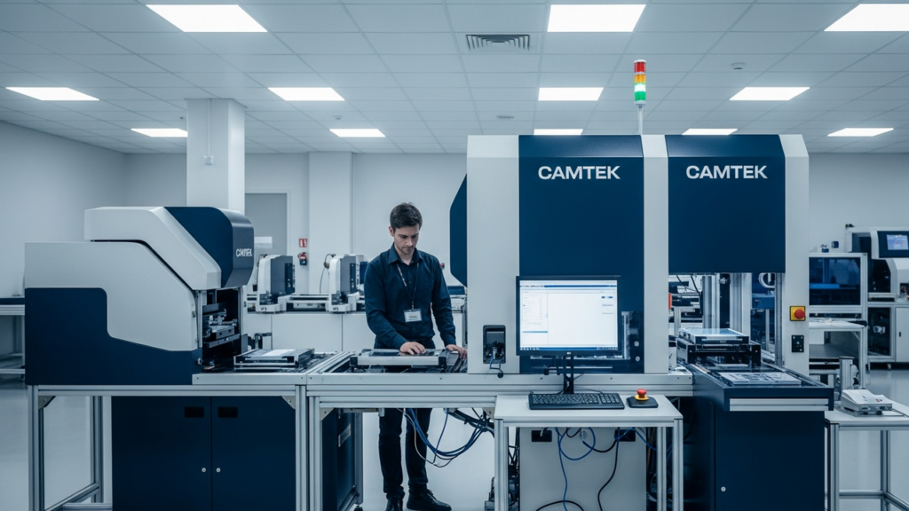
Camtek’s Precision Inspection and Metrology Solutions Drive Yield and Efficiency in Advanced Packaging
Camtek イスラエル Overview Camtek provides industry-leading 2D and 3D inspection and metrology platforms that address the escalating complexity and rapid growth of the advanced packaging market. Featuring sub-micron defect detection, CAD...


1