Samsung Electronics– tag –
-

Samsung Dedicates Half of Its 4nm Foundry Capacity to HBM4 Base Dies Amid AI Boom
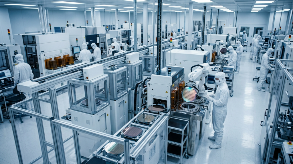
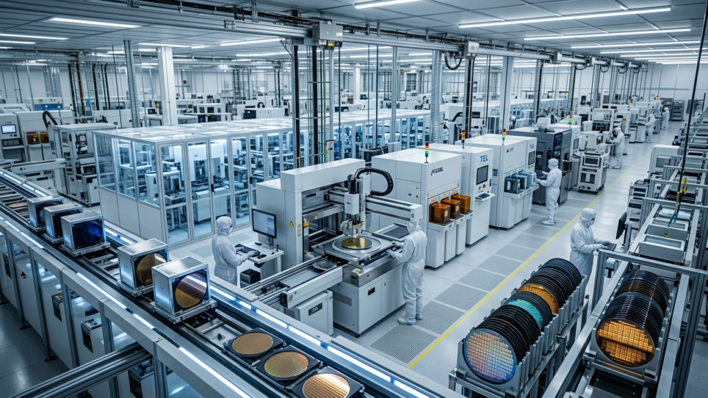
ZDNet Korea South Korea Overview Samsung Electronics is reportedly allocating over 50% of its advanced 4nm foundry capacity—specifically 15,000 wafers per month out of an estimated 30,000 total—to the production of HBM4 base dies. This s... -
Micron Reportedly Targets Doubling HBM Capacity to 100,000 Wafers/Month by End-2026, Boosting 12-High HBM4 for NVIDIA Vera Rubin
digitimes USA Overview Micron is reportedly targeting a near-doubling of its High Bandwidth Memory (HBM) production capacity to approximately 100,000 wafers per month by the end of 2026. This significant expansion focuses on ramping up p... -
Samsung Electro-Mechanics Unveils Five Next-Gen Semiconductor Package Substrate Products for AI, Automotive, and Mobile Markets at KPCA Show
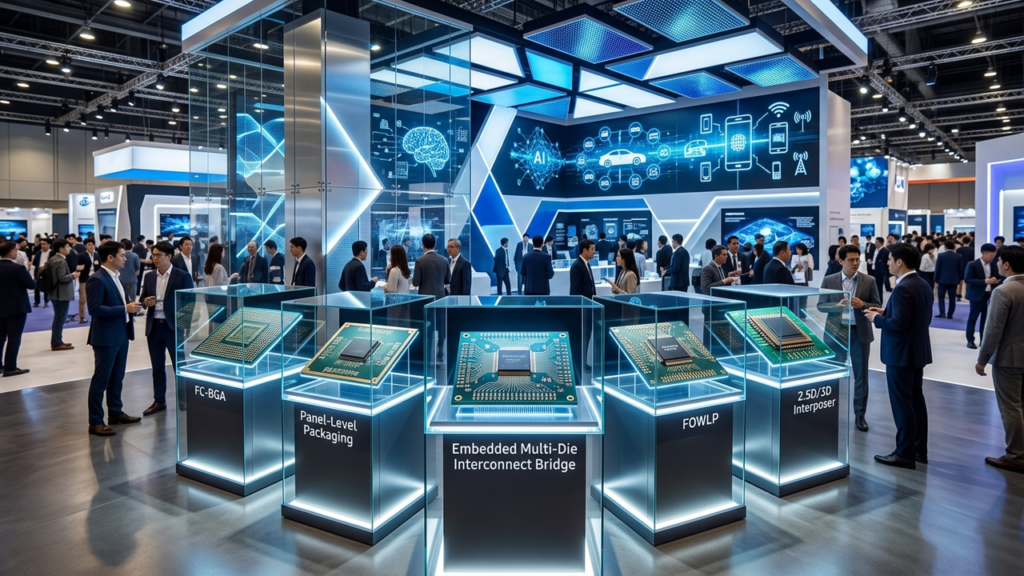
Global Sources South Korea Overview Samsung Electro-Mechanics showcased next-generation semiconductor package substrate technologies at KPCA Show, targeting high-end chip applications like AI servers, automotive systems, and mobile devic... -
Samsung Unveils 3D-Stacked Memory Strategy, Featuring HBM5, zHBM, and zNAND-O, to Break AI’s Memory Wall
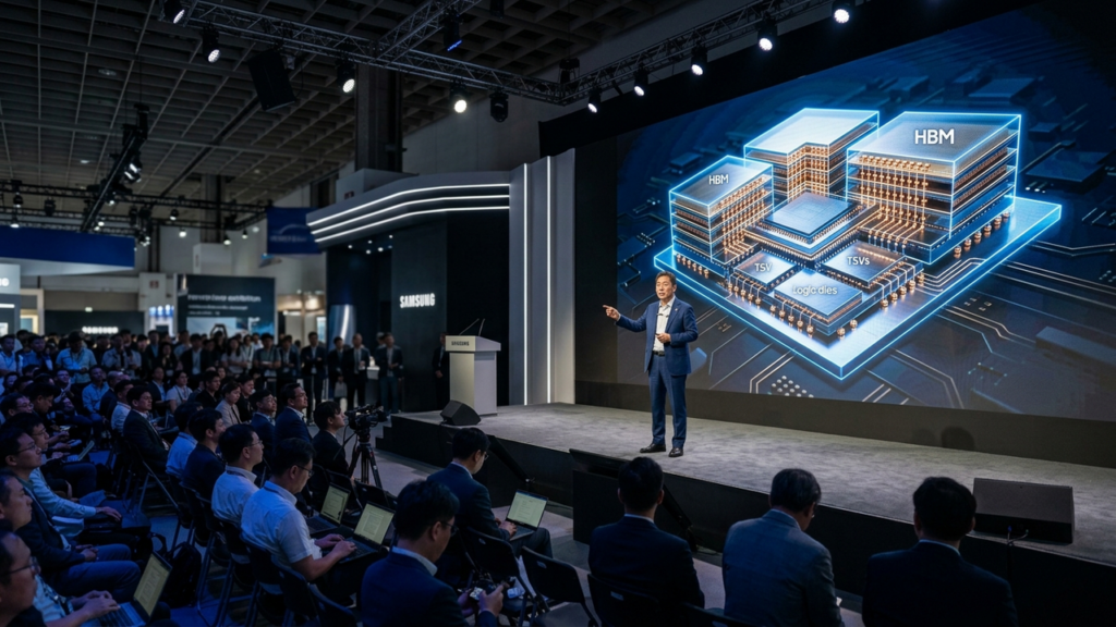
Design And Reuse South Korea Overview At SEMICON Taiwan 2026, Samsung Electronics presented a bold 3D-stacked memory strategy designed to overcome the limitations of current memory architectures in the AI era. This roadmap introduces HBM... -
Samsung Electronics Establishes Advanced Packaging R&D Center in Yokohama to Deepen Collaboration with Japanese Suppliers for HBM Technologies
digitimes South Korea Overview Samsung Electronics has opened an advanced packaging research center in Yokohama, Japan, to strengthen development cooperation with Japanese suppliers of critical materials and equipment for HBM. This strat... -
NVIDIA to Boost CoWoS Production Capacity by 3.5x to Over 120,000 Wafers/Month by End-2026, Securing HBM4 Supply
SemiconductorX USA Overview NVIDIA plans to scale its CoWoS (Chip-on-Wafer-on-Substrate) production capacity by 3.5x to 120,000–130,000 wafers per month by the end of 2026, up from 35,000, driven largely by its own demand. The company is... -
Samsung Foundry Unveils Next-Gen HBM Architecture Leveraging Advanced Packaging for AI/HPC Performance
Samsung Foundry South Korea Overview Samsung Foundry announced a new HBM architecture that combines advanced logic nodes with advanced packaging, promising significantly higher bandwidth and energy efficiency for AI and HPC systems. Its ... -
US Trade Policy and BIOSECURE Act Drive Major Reshaping and Investment in Global ADC Manufacturing Landscape
Bioprocess Online USA Overview U.S. trade policy and the BIOSECURE Act are significantly reshaping the Antibody-Drug Conjugate (ADC) manufacturing landscape, spurring substantial investments in capacity across the U.S., Europe, and Asia.... -
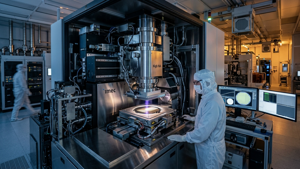
Imec Unlocks 22nm Pitch Single Patterning for High NA EUV Lithography, Accelerating Next-Gen Microchip Manufacturing
imec Belgium Overview Imec has announced a significant advancement in high-NA extreme ultraviolet (EUV) lithography, extending chemically amplified resists to enable single patterning of 22nm pitch line structures. This breakthrough is c... -
Mistral AI Secures €3 Billion in Samsung Electronics-Led Round, Valuation Soars Past €21 Billion, Forges Semiconductor AI Partnership
The Korea Herald South Korea Overview French AI startup Mistral AI raised €3 billion (approximately $3.5 billion) in a funding round led by Samsung Electronics and EQT’s Scale-Up Europe Fund, pushing its valuation beyond €21 billion. Thi...