Stacking– tag –
-

Taiyo Holdings Launches Next-Gen Semiconductor Packaging Material ‘FPIM Series,’ First to Achieve 700nm CD Three-Layer RDL on 12-inch Wafers
PR Newswire Japan Overview Taiyo Holdings, in collaboration with imec, has launched its "FPIM Series," a next-generation semiconductor packaging material that enables the first successful formation of a three-layer Redistribution Layer (... -
Panel Warpage Control Emerges as Key Bottleneck Hindering FOPLP Cost Advantage in Advanced Packaging
EAA Partners - Substack USA Overview Panel warpage control is identified as a critical bottleneck preventing Fan-Out Panel Level Packaging (FOPLP) from realizing its theoretical cost advantages in advanced semiconductor manufacturing. Th... -
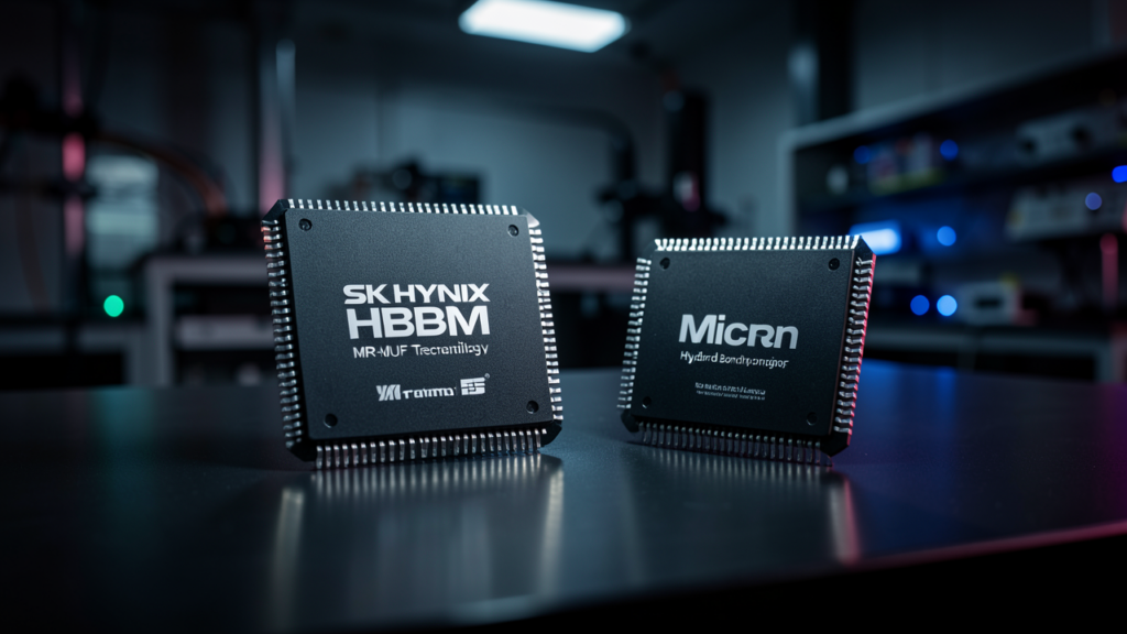
SK Hynix Breakthrough: Mass Reflow Underfill Molding Overcomes HBM Stacking Thermal Challenges, While Micron’s Hybrid Bonding Slashes Power Consumption by 30%
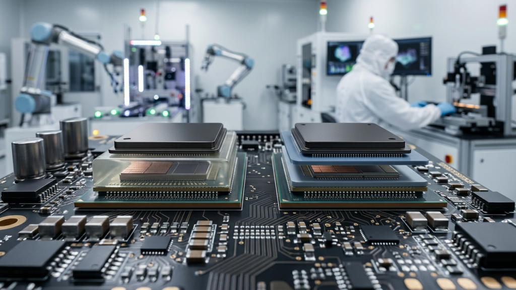
CSIS USA Overview SK Hynix has established a lead in HBM chip stacking by investing heavily in 'Mass Reflow Underfill Molding' (MR-MUF), a novel packaging technique that resolves the thermal and physical constraints of multi-die HBM stac... -
SK hynix’s MR-MUF and Samsung’s TC-NCF Revolutionize Thermal Management in AI Semiconductor HBM: Driving Advanced Packaging Evolution
USD Analytics Global Overview The evolution of AI is driving significant changes in semiconductor packaging and High Bandwidth Memory (HBM) technologies, with SK hynix's Advanced MR-MUF and Samsung's TC-NCF technologies solving critical ... -
Henkel Unveils Technomelt AS 4004 Hot-Melt Adhesive: Low Processing Temperature Solution Prevents Roof Tile Transport Damage
SpecialChem Germany Overview Henkel has launched Technomelt AS 4004, a new polypropylene-based hot-melt adhesive designed to prevent transport damage on roof tiles. This adhesive operates at a lower processing temperature than traditiona... -
Applied Materials Unveils Material Engineering Systems for Next-Gen AI Chips Featuring Advanced 3D Architectures
YouTube (Applied Materials channel) USA Overview Applied Materials has introduced a new suite of chipmaking systems designed to enable advanced 3D chip architectures for next-generation AI. The company is facilitating this transition thr... -
Intel Foundry Leverages U.S. Advanced Packaging (Foveros, EMIB) to Power Next-Gen AI Semiconductors
Intel Newsroom USA Overview Intel Foundry is accelerating the realization of next-generation AI semiconductors through its advanced packaging technologies developed in U.S. facilities. Utilizing Foveros stacking, EMIB silicon bridges, an... -
Qnity Electronics Accelerates AI-Centric Advanced Packaging R&D with Expanded imec Collaboration
Converge Digest Belgium Overview Qnity Electronics has significantly expanded its strategic collaboration with imec, a world leader in nanoelectronics, to bolster long-term R&D in advanced semiconductor packaging crucial for AI and h... -
Sheen Technology Details Evolving TIM Requirements for AI Chips, Emphasizing High Thermal Conductivity and Low Thermal Resistance for Liquid Cooling
Sheen Technology Taiwan Overview Sheen Technology has published a comprehensive guide outlining the evolving requirements for Thermal Interface Materials (TIMs) in high-performance AI chips. Driven by advanced packaging such as 2.5D/3D s... -
SK Hynix to Launch Advanced Packaging Plant in Indiana, USA by H2 2028 to Meet Surging HBM3 Demand
BigGo Finance South Korea Overview SK hynix is driving aggressive capacity expansion to meet the surging demand for High Bandwidth Memory 3 (HBM3). The company plans to begin operations at an advanced packaging plant in Indiana, USA, by ...








12