Background: The Imperative for Advanced Packaging
As the semiconductor industry grapples with the slowing pace of Moore’s Law, advanced packaging technology has emerged as a critical frontier for driving chip performance enhancements and cost efficiencies. High-performance interposers are indispensable for realizing the full potential of chiplet architectures and 3D-ICs, enabling heterogeneous integration and increased functional density. Among various contenders, glass substrates have rapidly gained prominence as a compelling candidate for these next-generation interposers. Their inherent material properties offer distinct advantages over traditional organic or silicon alternatives.
Global investments in glass substrate technology are escalating, with significant research and development efforts underway in regions such as the U.S. and South Korea. Against this backdrop, imec’s latest breakthrough underscores Europe’s strategic position and potential to lead in this pivotal technological race, promising to reshape the future of semiconductor integration for demanding applications like AI and High-Performance Computing (HPC).
A Major Step Forward in Glass-Based 3D Packaging
imec, the world-leading microelectronics research institute headquartered in Belgium, has unveiled a pivotal technological breakthrough in 3D stacked packaging utilizing glass substrates. This highly anticipated development is poised to significantly advance the creation of higher-performance and more power-efficient integrated circuits, particularly for Artificial Intelligence (AI) and High-Performance Computing (HPC) applications.
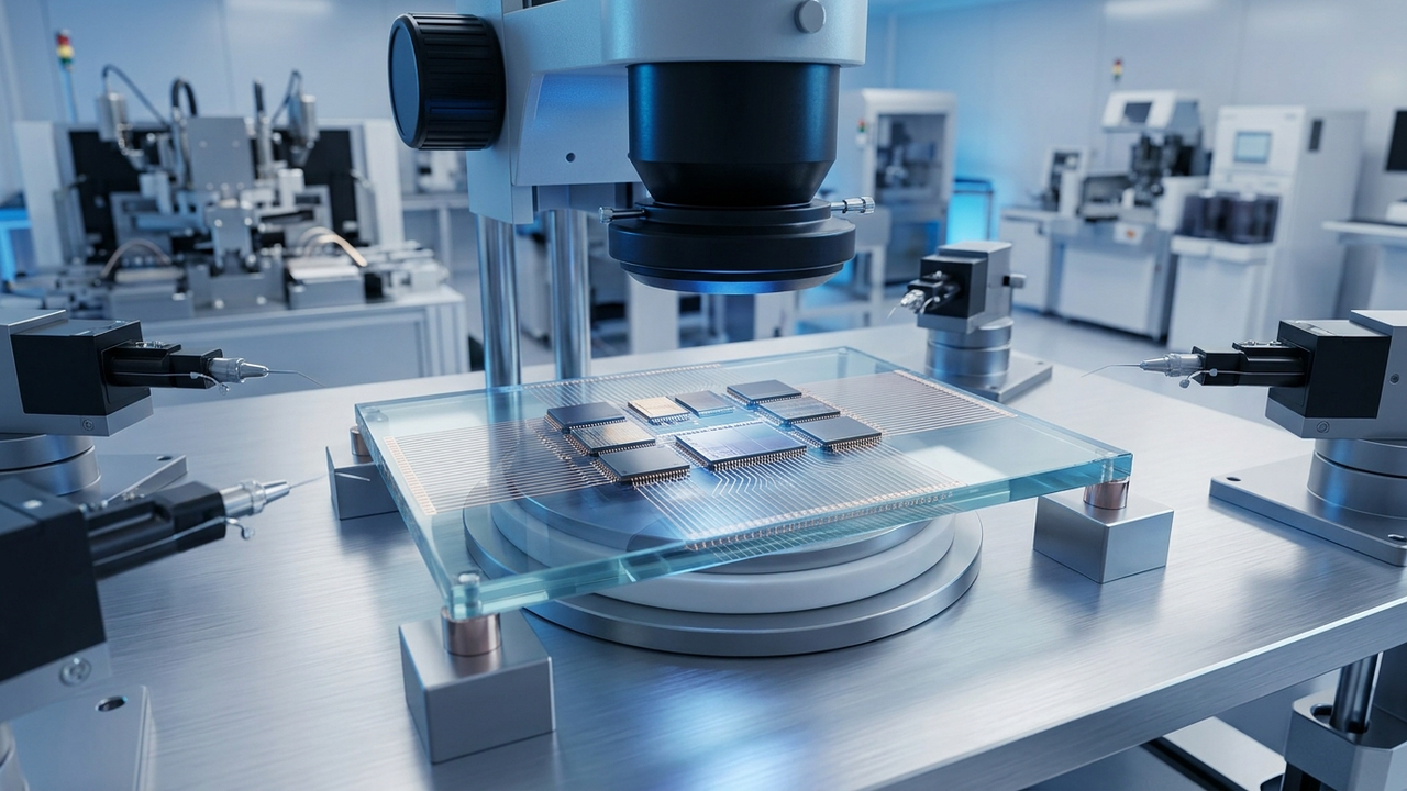
Glass substrates present several compelling advantages over incumbent organic or silicon interposers. Key benefits include superior intrinsic flatness, exceptionally low dielectric loss, high thermal stability, and an inherent suitability for fine-pitch processing. These attributes are critical for enabling ultra-high-density integration of diverse chiplets and High Bandwidth Memory (HBM), facilitating faster signal propagation, reducing parasitic capacitance, and ultimately lowering overall power consumption. imec’s achievement represents a substantial stride towards the commercialization of this innovative technology, drawing significant interest across the semiconductor ecosystem.
Technical Innovations Enabling the Breakthrough
imec’s significant advancements in 3D stacked packaging with glass substrates are underpinned by several critical technical innovations:
- Ultra-Fine Through-Glass Via (TGV) Technology: imec has successfully established precise control over sidewall etching and achieved high aspect ratios in the formation of Through-Glass Vias. This breakthrough overcomes previous manufacturing challenges, ensuring exceptionally high wiring density and superior electrical performance essential for high-speed data transfer.
- Low-Warpage and High-Reliability Processing: Novel processing techniques have been developed to effectively mitigate warpage during the handling and fabrication of large-format glass substrates. This control is crucial for enhancing manufacturing yield during subsequent chip stacking operations and significantly improving overall package reliability and longevity.
- Advanced Heterogeneous Integration Capabilities: imec has pioneered technologies for the efficient integration of a diverse array of chiplets—including logic, memory, and RF components—fabricated using disparate materials and processes, onto a single glass interposer. This capability is fundamental for constructing complex, high-performance System-in-Packages (SiPs).
- Synergy with Electro-Optical Integration: Beyond electrical interconnects, imec is also actively researching the fabrication of optical waveguides and components directly on glass substrates. This foresight anticipates the future integration of optical interconnects, paving the way for even higher bandwidth and lower power communication within advanced packages.
To accelerate the practical application of these technologies, imec is actively engaged in collaborative R&D efforts with a consortium of leading industry partners, including major semiconductor manufacturers and equipment suppliers.
Industry Impact and Future Outlook
imec’s pioneering 3D stacked packaging technology, leveraging glass substrates, is projected to find critical applications within the next few years across high-demand sectors such as AI/HPC processors, high-performance network infrastructure, and advanced autonomous driving systems. The accelerated commercialization of this technology promises to dramatically enhance chip design flexibility, facilitating the development of increasingly complex and high-performance System-in-Package (SiP) solutions.
Looking ahead, imec is committed to the continuous development of this foundational technology, driving innovation across the broader semiconductor industry. By providing key enabling technologies, imec aims to support and shape the evolution of next-generation electronics, ensuring sustained advancements in performance, power efficiency, and functionality for the most challenging computing tasks.
Source: #
Get our weekly technology intelligence — free
Receive an infographic that lets you judge at a glance whether each field’s analysis report is worth reading.
Subscribe Free — Weekly Tech Intelligence
By subscribing, you’ll receive Troy-Technical’s weekly technology intelligence newsletter.
- Your email and selected fields are used only to deliver the newsletter.
- We never share your information with third parties.
- You can unsubscribe anytime via the link in each email.
See our Privacy Policy for details.
Takes about a minute · Unsubscribe anytime









Comments