Key Findings
Glass substrates are emerging as a pivotal breakthrough technology for next-generation AI chip packaging, with industry leaders such as Intel, TSMC, and Samsung Electro-Mechanics significantly accelerating their development efforts. Glass substrates offer the potential to support larger package sizes, finer interconnects, and higher connection densities compared to conventional organic substrates. Particularly, their coefficient of thermal expansion (CTE) closely matches that of silicon, which is highly valued for dimensional stability in large-scale chiplet integration, promising enhanced performance and cost reduction for AI and High-Performance Computing (HPC) chips.
Technical & Clinical Details
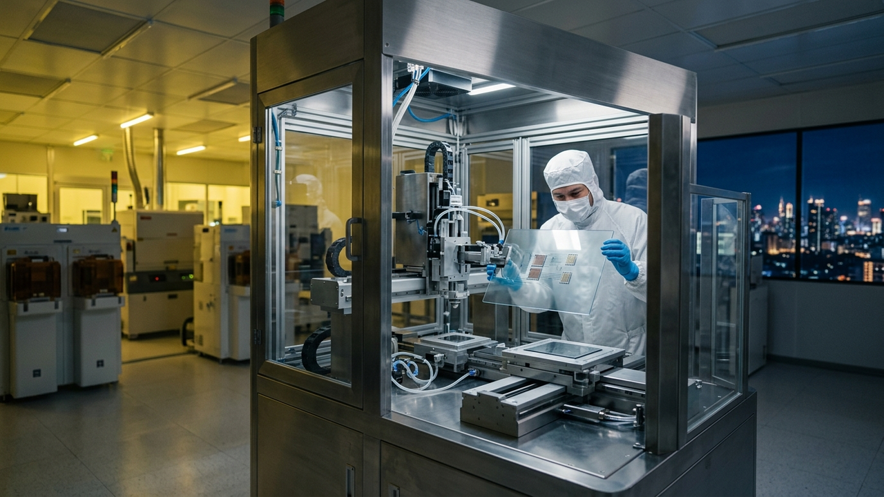
The primary advantages of glass substrates lie in their superior mechanical strength, thermal stability, and low dielectric loss characteristics. These properties enable the formation of finer line/space (L/S) wiring and high-density Through-Glass Vias (TGVs). TGVs are minute electrical interconnections passing through the glass substrate, facilitating high-speed, low-latency data transmission between chiplets and High Bandwidth Memory (HBM).
Intel announced its glass core substrate as an alternative to organic chip packaging in September 2023, which is currently in the final qualification stages. Absolics, a subsidiary of SKC, is conducting package-level reliability evaluations for glass substrates produced at its Georgia factory in Taiwan, with results expected by year-end. Samsung Electro-Mechanics and LG Innotek are also advancing their glass substrate programs, and Dai Nippon Printing aims for full-scale mass production by 2028. A significant manufacturing challenge involves reliably coating millions of TGVs; TRUMPF has introduced a High Power Impulse Magnetron Sputtering (HiPIMS) approach to form more uniform conductive coatings inside deep, narrow holes, aiming to resolve this bottleneck.
Background & Context
The explosive demand for AI chips is pushing the boundaries of traditional packaging technologies. The strain on TSMC’s CoWoS capacity and the HBM supply shortage have underscored the critical need for alternative, advanced packaging materials. Glass substrates are rapidly gaining industry attention as a promising candidate to address these challenges. Especially with the proliferation of chiplet architectures and heterogeneous integration, the CTE mismatch between different materials profoundly affects package reliability and yield. The silicon-like CTE of glass substrates mitigates this issue, enabling the realization of larger, higher-performance AI chips. Government policies, such as the CHIPS Act in various countries, are also supporting the development of advanced packaging technologies and strengthening domestic manufacturing capabilities, thereby accelerating investment in glass substrate development.
Strategic Significance & Outlook
Glass substrates are establishing their technological superiority en route to full-scale commercialization, projected for 2028 and beyond. Should companies like Absolics complete their reliability evaluations, adoption by major chip manufacturers, including Intel, could accelerate. Innovations in manufacturing processes, such as TRUMPF’s HiPIMS technology, are indispensable for overcoming key bottlenecks in glass substrate mass production and enhancing cost efficiency. The widespread adoption of glass substrates is expected to further boost AI chip performance, enabling new breakthroughs across a wide range of applications, from data centers to edge AI devices. This will likely propel the semiconductor industry into its next phase of growth.
Source: https://www.nepconasia.com/en-gb/media/press-release/2026/9/1.html
Get our weekly technology intelligence — free
Receive an infographic that lets you judge at a glance whether each field’s analysis report is worth reading.
Subscribe Free — Weekly Tech Intelligence
By subscribing, you’ll receive Troy-Technical’s weekly technology intelligence newsletter.
- Your email and selected fields are used only to deliver the newsletter.
- We never share your information with third parties.
- You can unsubscribe anytime via the link in each email.
See our Privacy Policy for details.
Takes about a minute · Unsubscribe anytime









Comments