Key Findings
KLA is experiencing substantial benefits from the escalating demand for inspection, metrology, and process control solutions in advanced packaging, driven by the increasing complexity of AI and High-Performance Computing (HPC) chips and the progression of hybrid bonding technologies. The company’s advanced packaging business is projected to achieve over 70% revenue growth in 2026, reaching approximately $1.1 billion. This growth is directly attributable to the critical need for KLA’s technology to identify defects in early manufacturing stages and prevent expensive production losses, especially as the economic impact of defects in multi-die integrated packages like chiplets and High Bandwidth Memory (HBM) dramatically increases.
Technical & Clinical Details
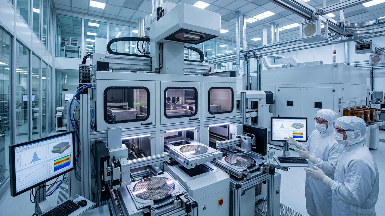
AI and HPC chips often employ heterogeneous integration, involving the complex arrangement of multiple chiplets and memory dies both vertically and horizontally. In such intricate setups, even minute defects during the packaging process can lead to final product failure or significant yield degradation. To address these advanced packaging challenges, KLA offers a comprehensive portfolio of process control platforms, including sophisticated optical inspection systems, high-precision dimensional metrology tools, and chemical analysis solutions for material characterization.
Emerging interconnect technologies like hybrid bonding (direct copper-to-copper bonding) enable higher connection densities and shorter signal paths. However, they also impose extremely tight manufacturing tolerances, making microscopic particles or alignment errors catastrophic. KLA’s systems provide high-resolution defect detection capabilities and real-time process feedback to manage these challenges effectively. Similar to Onto Innovation’s Dragonfly G5 platform being adopted for HBM4 and 2.5D AI packaging, and Camtek’s surging orders for advanced packaging inspection, KLA maintains a strong market position with its broad portfolio.
Background & Context
As AI drives transformations across both ends of the semiconductor manufacturing process, KLA is meeting market needs through its extensive range of process control platforms. The increasing size and layer count of AI chip designs significantly escalate manufacturing costs and timelines, making the economic loss from a single defect substantial. Consequently, the value of rigorous inspection and metrology at every stage of the manufacturing process has dramatically increased. With governments, including those implementing the U.S. CHIPS Act, focusing on semiconductor supply chain resilience and domestic manufacturing capacity, process control equipment suppliers like KLA play a strategically vital role due to their indispensable contribution to manufacturing efficiency and yield improvement.
Strategic Significance & Outlook
The evolution of AI chips is relentless, and packaging complexity will only continue to grow. The introduction of technologies such as glass substrates and novel interconnects will demand even more sophisticated inspection and metrology capabilities. KLA, leveraging its broad portfolio and extensive expertise, is expected to maintain its leadership in process control within the advanced packaging market, even as competition intensifies with rivals like Onto Innovation and Applied Materials. Future technological developments for KLA will likely focus on enhancing defect detection precision, incorporating AI-driven data analysis, and enabling automated process optimization. These advancements are crucial for reducing AI chip manufacturing costs and accelerating time-to-market, thereby serving as a critical foundation for the overall growth of the AI industry.
Source: https://qz.com/kla-gains-from-advanced-packaging-can-it-outpace-onto-amat
Get our weekly technology intelligence — free
Receive an infographic that lets you judge at a glance whether each field’s analysis report is worth reading.
Subscribe Free — Weekly Tech Intelligence
By subscribing, you’ll receive Troy-Technical’s weekly technology intelligence newsletter.
- Your email and selected fields are used only to deliver the newsletter.
- We never share your information with third parties.
- You can unsubscribe anytime via the link in each email.
See our Privacy Policy for details.
Takes about a minute · Unsubscribe anytime









Comments