
Key Findings
Google and Marvell announced a strategic collaboration on custom silicon programs designed to interface with Google’s Tensor Processing Unit (TPU) ecosystem. Concurrently, Marvell significantly increased its fiscal year 2027 revenue outlook for scale-up optics, emphasizing the central role of optical communication technology in AI infrastructure. Furthermore, Ayar Labs successfully demonstrated an astonishing 8 Tbps optical I/O chiplet, and Marvell acquired Celestial AI to launch its Photonic Fabric memory line, which combines optical Systems-on-Chip (SoCs) with High Bandwidth Memory (HBM) cache, poised to fundamentally transform data center performance in the AI era.
Technical / Clinical Details
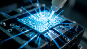
The Google-Marvell partnership suggests that advanced optical interconnects will be indispensable for next-generation TPU architectures. Marvell’s ‘scale-up optics,’ projected for substantial revenue growth, refers to a suite of technologies designed to integrate multiple ASICs or GPUs and accelerate data transfer. Ayar Labs’ demonstrated 8 Tbps optical I/O chiplet holds the potential to deliver petabit-scale bandwidth over a single optical interface, drastically reducing power consumption compared to traditional electrical wiring. Marvell’s acquisition of Celestial AI and the launch of its Photonic Fabric memory line represent a strategic push towards Co-Packaged Optics (CPO) and chiplet approaches that directly integrate optical technology with processors and memory. This strategy aims to eliminate data transfer bottlenecks and enable efficient communication between AI accelerators, thereby dramatically improving AI workload training speeds and inference performance.
Background & Context
The rapid evolution of AI and HPC has placed unprecedented demands not only on data center compute capacity but also on the bandwidth and power efficiency of the underlying data transfer. Particularly, data transfers within large GPU clusters and between AI accelerators have reached limitations with conventional copper cabling and pluggable optical modules, exacerbating issues of power consumption and heat. Against this backdrop, there is growing interest in ‘In-Package Optics’ and ‘Co-Packaged Optics’ technologies that integrate optical components directly onto the chip. Strategic moves by industry leaders like Marvell and Google in this domain strongly indicate that optical technology is the next frontier for AI infrastructure.
Strategic Significance & Outlook
These strategic partnerships, acquisitions, and technology demonstrations hold profound implications for shaping the future of AI and high-performance computing. Marvell’s Photonic Fabric memory line and Ayar Labs’ 8 Tbps chiplet are expected to accelerate AI innovation by resolving data transfer bottlenecks and improving power efficiency as AI models grow in size and complexity. With optical communication integrated down to the chip level, data centers will evolve into higher-performance and more sustainable infrastructures, opening new possibilities in fields such as autonomous driving, medical AI, and scientific simulations. This trend is set to blur the lines between semiconductors and optical communications, ushering in a new era of competition and collaboration across the industry.
Source: https://fundaai.substack.com/p/deepoptics-scale-in-moves-optics
Get our weekly technology intelligence — free
Receive an infographic that lets you judge at a glance whether each field’s analysis report is worth reading.
Subscribe Free — Weekly Tech Intelligence
By subscribing, you’ll receive Troy-Technical’s weekly technology intelligence newsletter.
- Your email and selected fields are used only to deliver the newsletter.
- We never share your information with third parties.
- You can unsubscribe anytime via the link in each email.
See our Privacy Policy for details.
Takes about a minute · Unsubscribe anytime





Comments