Key Findings
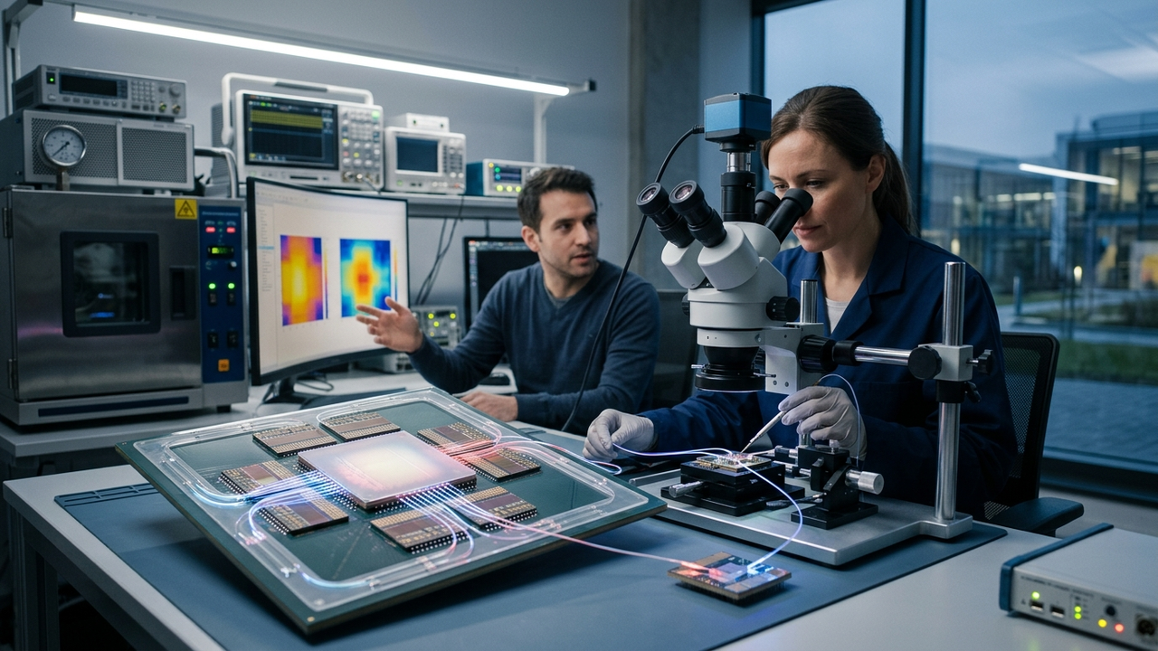
Semiconductor Engineering reported that the integration of photonics is necessitating a fundamental rethinking of chiplet design. This evolution is driven by the bidirectional interaction of thermal, mechanical, electromagnetic, and optical effects, transforming chiplet design from a mere placement challenge into a complex multi-physics co-design problem.
Technical / Clinical Details
Approaches like Co-Packaged Optics (CPO) and In-Package Optics, which tightly integrate optical chiplets with computational silicon, promise significant improvements in data transmission bandwidth and power efficiency. However, this integration introduces new design challenges. For example, heat generated by an optical chiplet can impact the performance of adjacent computational silicon, and vice versa. Discrepancies in thermal expansion coefficients between chiplets made of different materials can induce mechanical stress, potentially compromising optical alignment stability and long-term reliability. Consequently, designers must adopt a ‘multi-physics co-design’ framework that simultaneously considers thermal, stress, electromagnetic, and optical characteristics. TSMC’s Compact Universal Photonic Engine (COUPE), announced for the mass production of optical chiplets, is an advanced packaging platform designed to address these complex challenges by integrating precise alignment and thermal management technologies.
Background & Context
The explosive growth of data processing in AI, High-Performance Computing (HPC), and cloud data centers has exposed the limitations of traditional electrical interconnects. Electrical wiring has become a bottleneck in terms of bandwidth, power consumption, and signal loss, impeding the scalability of next-generation systems. In contrast, optical communication offers a promising solution for ultra-high-speed, low-power data transfer, but the process of integrating optical components directly with semiconductor chips is exceedingly complex. Chiplet architectures aim to enhance flexibility and efficiency by combining smaller chips with different functionalities, but the introduction of photonics chiplets adds a new dimension of complexity to this design paradigm.
Strategic Significance & Outlook
The shift towards multi-physics co-design for photonics chiplets will accelerate the evolution of semiconductor design tools and necessitate new expertise in heterogeneous integration. Platforms like TSMC’s COUPE will play a critical role in simplifying this complex integration process and enabling the mass production of optical chiplets. This will allow AI accelerators and network switches to achieve higher bandwidth density, superior power efficiency, and lower latency. Ultimately, this technological innovation is expected to dramatically enhance AI computational capabilities, support the sustainable growth of data centers, and open up new application possibilities in areas such as autonomous driving, medical diagnostics, and scientific research. The convergence of semiconductors and optical communications will be an indispensable element in shaping the future of digital technology.
Source: https://semiengineering.com/photonics-forces-a-chiplet-rethink/
Get our weekly technology intelligence — free
Receive an infographic that lets you judge at a glance whether each field’s analysis report is worth reading.
Subscribe Free — Weekly Tech Intelligence
By subscribing, you’ll receive Troy-Technical’s weekly technology intelligence newsletter.
- Your email and selected fields are used only to deliver the newsletter.
- We never share your information with third parties.
- You can unsubscribe anytime via the link in each email.
See our Privacy Policy for details.
Takes about a minute · Unsubscribe anytime





Comments