Background & Context
The relentless expansion of AI applications has fueled an unprecedented demand for high-performance, efficiently manufactured AI semiconductors. Advanced packaging technologies like Panel-Level Packaging (PLP) are now indispensable for overcoming the physical and electrical limitations of traditional methods, enabling greater integration density, reduced latency, and improved power efficiency. With AI accelerators requiring massive data processing capabilities, sophisticated high-density packaging capable of accommodating chiplets and High Bandwidth Memory (HBM) stacks is paramount. Powertech’s investment represents a strategic response to this critical market imperative, reinforcing Taiwan’s leading position in the global semiconductor ecosystem and mitigating potential supply chain bottlenecks for critical AI components, a challenge recently observed in CoWoS packaging capacity.
Key Announcements
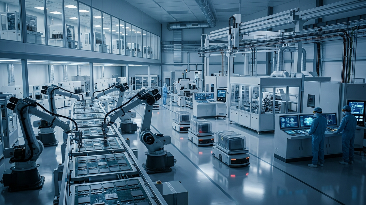
Powertech Technology (PTI), a prominent Taiwanese Outsourced Semiconductor Assembly and Test (OSAT) provider, has announced its strategic plan to commence mass production of panel-level packaging (PLP) services for artificial intelligence (AI) semiconductors and server CPUs by early 2027. This initiative marks a significant milestone, as the facility is anticipated to be the world’s first large-scale PLP operation specifically dedicated to AI chip manufacturing, directly addressing the critical demand for advanced packaging solutions in the booming AI sector.
Technical Deep Dive into Panel-Level Packaging (PLP)
Panel-level packaging (PLP) represents a next-generation approach to semiconductor packaging, distinguishing itself from traditional wafer-level packaging (WLP) by utilizing large, rectangular panels instead of smaller, circular silicon wafers. This methodology allows for a substantially increased number of chips to be processed simultaneously, leading to significant enhancements in production throughput and cost efficiency, particularly beneficial for large-die AI processors and High-Performance Computing (HPC) semiconductors. PTI’s adoption of PLP technology is poised to deliver high-density, high-performance packaging solutions, which are crucial for advanced AI chips that frequently integrate High Bandwidth Memory (HBM) and complex 2.5D/3D architectures. The larger panel size, potentially up to 600mm x 600mm, facilitates a higher package-per-panel ratio, drastically improving overall processing economics compared to conventional 300mm wafer-based methods.
Strategic Significance & Outlook
The commencement of PLP mass production by Powertech is expected to significantly expand the global supply capacity for AI semiconductors, thereby accelerating the development and deployment of AI technologies across diverse industries. Furthermore, PTI’s pioneering initiative could catalyze broader industry adoption of PLP, encouraging other OSAT providers and foundries to invest in similar advanced packaging capabilities. This trend is likely to lead to a reduction in per-chip costs for AI processors and facilitate their integration into a wider array of applications, spanning from edge devices to hyperscale data centers. Powertech is strategically positioned to remain a pivotal player in driving the growth of the AI semiconductor market, with its advancements closely monitored by industry stakeholders, potentially establishing a new benchmark for advanced packaging efficiency and scalability.
Source: https://tonarism.co.jp/media/media_detail.php?b_id=261
Get our weekly technology intelligence — free
Receive an infographic that lets you judge at a glance whether each field’s analysis report is worth reading.
Subscribe Free — Weekly Tech Intelligence
By subscribing, you’ll receive Troy-Technical’s weekly technology intelligence newsletter.
- Your email and selected fields are used only to deliver the newsletter.
- We never share your information with third parties.
- You can unsubscribe anytime via the link in each email.
See our Privacy Policy for details.
Takes about a minute · Unsubscribe anytime









Comments