


Key Findings
Qualcomm and Huawei entered a multi-year, broad patent licensing agreement on October 5, covering 5G, computing, artificial intelligence, and networking. While Qualcomm is acquiring specific non-cellular US patents from Huawei, the company explicitly refuted claims that it has become a net payer to Huawei. Furthermore, Qualcomm denied that the agreement involves licenses for Huawei’s “Logic Folding” chip technology, contradicting earlier reports from Bloomberg and Shenzhen TV’s “Shenzhen News.”
Technical Details of Logic Folding
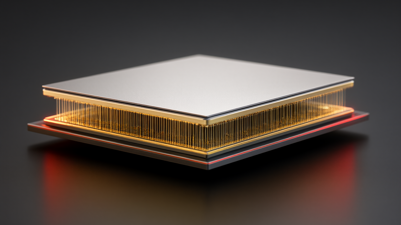
Logic Folding is a technology path within Huawei’s “Tau Scaling Law” framework, introduced by He Tingbo at the IEEE ISCAS 2026 conference. The approach aims to circumvent EUV lithography restrictions by compressing signal delay through vertical stacking rather than transistor shrinking. Key technical specifications include:
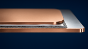
- Architecture: Two bonded active dies working as a single unit using copper-to-copper hybrid bonding.
- Interconnects: A 1.5-micron hybrid bonding pitch with approximately 50 million interconnect points.
- Performance Gains: Wire length is reduced by 30%, core routing by 20%, and critical paths by up to 70%.
- Efficiency: At equivalent performance, power consumption is reduced by 66% for the NPU, 58% for the GPU, and 41% for CPU performance cores.
Implementation in Kirin 9050 Pro
The technology is implemented in the Kirin 9050 Pro chip found in the Mate XT 2 tri-fold phone. Die-level teardowns reveal a face-to-face bonded structure where the upper die contains high-density compute units (CPU execution units, GPU, NPU logic), while the lower die houses the L3 cache, 12MiB system cache, PLL, and I/O interfaces (LPDDR, PCIe, USB). The combined die area exceeds 240 square millimeters, with transistor density increasing to 238 MTr/mm² from 155 MTr/mm².
Significance and Outlook
The controversy over the licensing terms underscores the industry’s interest in Huawei’s ability to maintain performance via 3D stacking. While the official agreement remains confidential, the denial of “Logic Folding” licenses suggests that this specific architectural path remains proprietary to Huawei.
Source: https://finance.biggo.com/news/6520ef39-1dd1-400a-ab83-9290855da6ee
Get our weekly technology intelligence — free
Receive an infographic that lets you judge at a glance whether each field’s analysis report is worth reading.
Subscribe Free — Weekly Tech Intelligence
By subscribing, you’ll receive Troy-Technical’s weekly technology intelligence newsletter.
- Your email and selected fields are used only to deliver the newsletter.
- We never share your information with third parties.
- You can unsubscribe anytime via the link in each email.
See our Privacy Policy for details.
Takes about a minute · Unsubscribe anytime