


Key Findings
Researchers at the Karlsruhe Institute of Technology (KIT) have demonstrated a perovskite-silicon tandem cell with a maximum power conversion efficiency (PCE) of 30.2%. This marks the first time a tandem cell exceeding 30% efficiency has been achieved using an inkjet-printing-based process for the perovskite absorber deposition. The champion cell recorded an open-circuit voltage of 1.94 V, a short-circuit current density of 20.4 mA/cm², and a fill factor of 75.8%, maintaining efficiency above 30% during 10 minutes of maximum power point tracking.
Technical Details
The fabrication process utilizes a hybrid approach to deposit the various layers of the monolithic device:
- Hole Transport Layer (HTL): A self-assembled monolayer (SAM)-based HTL was deposited via dip-coating, using 2PACz for perovskite-only cells and Ph4PACz for tandem cells on textured silicon.
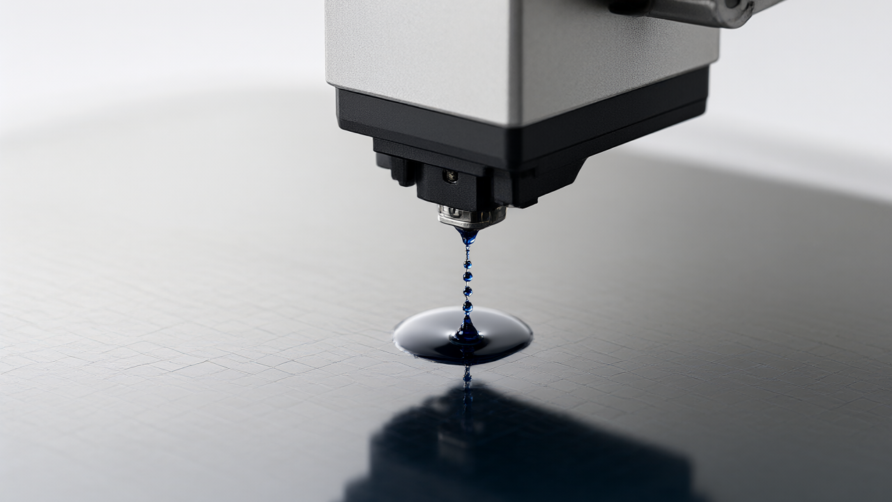
- Perovskite Absorber: A two-step hybrid process was employed, where inorganic precursors were first deposited by thermal evaporation, followed by the inkjet printing of organic precursors.
- Passivation: An interfacial passivation layer was applied above the perovskite absorber using dip-coating.
These layers were integrated with textured silicon heterojunction (HJT) bottom cells and a wide-bandgap perovskite top cell.
Scalability and Mini-Module Performance
To test the scalability of the process, the team developed a single-junction perovskite mini-module with an active area of 12.96 cm². The module consists of nine series-connected cell stripes (1.44 cm² each) created via laser scribing. This mini-module achieved a PCE of 17.8%, representing an efficiency loss of 0.53 percentage points per decade of area scaling compared to smaller cells.
Significance and Outlook
While the results validate the potential of inkjet printing and dip-coating for tandem cell production, the researchers noted that the fill factor of 75.8% indicates a need for further optimization of the tandem architecture on textured silicon surfaces. Future development will focus on improving process control and laser-scribing precision to transition this laboratory process into industrial manufacturing.
Source: https://taiyangnews.info/technology/kit-achieves-302-efficiency-in-inkjet-printed-tandem-cells
Get our weekly technology intelligence — free
Receive an infographic that lets you judge at a glance whether each field’s analysis report is worth reading.
Subscribe Free — Weekly Tech Intelligence
By subscribing, you’ll receive Troy-Technical’s weekly technology intelligence newsletter.
- Your email and selected fields are used only to deliver the newsletter.
- We never share your information with third parties.
- You can unsubscribe anytime via the link in each email.
See our Privacy Policy for details.
Takes about a minute · Unsubscribe anytime