


Key Findings
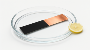
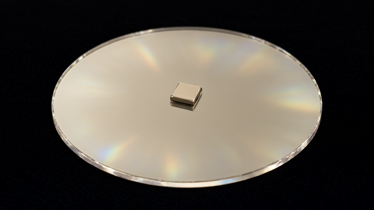
Diamond Foundry announced on November 5, 2026, the successful creation of a single crystal diamond with a diameter of 200mm. This represents a significant scale-up from the 100mm version released in October 2023. The company emphasizes that this is a continuous single crystal structure, rather than a polycrystalline diamond or a composite of smaller crystals.
Technical Details
The increase in diameter from 100mm to 200mm results in a theoretical area increase from approximately 78.5cm² to 314cm². This 200mm size aligns with the standard 8-inch wafer diameter used in the semiconductor industry. However, the company noted that the current achievement refers to unpolished material immediately after growth; polished substrates ready for semiconductor manufacturing have not yet begun shipping.
The development required advancements in several technical areas, including:
- Plasma control and chemical reactions during crystal growth.
- Reaction furnace design and temperature management.
- Measurement technology.
Background and Context
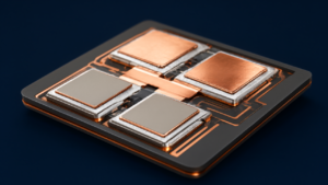
The breakthrough is the result of approximately 25 years of research by Stefan Gsell and Martin Fischer. Both joined Diamond Foundry following the company’s acquisition of Augsburg Diamond Technology in 2022. Single crystal diamond is targeted for AI GPU cooling due to its high thermal conductivity and electrical insulation, which help mitigate “hot spots” in high-power chips.
Significance and Outlook
While the material area has increased, Diamond Foundry cautions that actual cooling performance depends on the thermal resistance of the bonding layer between the chip and the diamond, as well as the external cooling mechanism. Data regarding defect density, yield, and effective diameter after processing have not been disclosed.
CEO Martin Roscheisen indicated that this milestone makes the production of 300mm single crystal diamonds technically foreseeable. However, specific timelines for mass production, pricing, and supply conditions for the 200mm material remain unspecified.
Source: https://xenospectrum.com/diamond-foundry-wafer-chip-cooling/
Get our weekly technology intelligence — free
Receive an infographic that lets you judge at a glance whether each field’s analysis report is worth reading.
Subscribe Free — Weekly Tech Intelligence
By subscribing, you’ll receive Troy-Technical’s weekly technology intelligence newsletter.
- Your email and selected fields are used only to deliver the newsletter.
- We never share your information with third parties.
- You can unsubscribe anytime via the link in each email.
See our Privacy Policy for details.
Takes about a minute · Unsubscribe anytime