Key Findings
Applied Materials has unveiled a new suite of chip manufacturing systems designed to enable the creation of advanced 3D chip architectures, crucial for empowering next-generation AI. These systems integrate the company’s material engineering expertise across DRAM, advanced packaging, and process control, aiming to help customers produce new generations of AI chips faster and with higher yields.
Technical Details
The new systems introduced by Applied Materials support AI chip manufacturing through the following technological innovations:
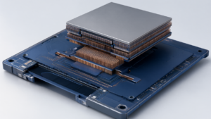
- Advanced 3D Chip Architectures: This technology involves vertically stacking multiple chips (such as DRAM and logic) to dramatically increase data bandwidth and reduce power consumption. This provides the high-speed data processing capabilities and efficiency essential for AI workloads.
- Optimized Material Engineering: Precise control over the properties of adhesives, sealants, and other materials used in advanced packaging processes ensures the stability and reliability of 3D structures. Interface adhesion and thermal management, particularly in heterogeneous integration of DRAM and logic, are critical aspects.
- High-Yield Production: The introduction of advanced process control systems reduces defect rates during manufacturing, enhancing the mass production yield of complex 3D AI chips. This leads to reduced manufacturing costs and accelerated time-to-market.
- Evolution of DRAM Technology: AI applications require vast amounts of data, making high-performance DRAM integration indispensable. Applied Materials’ systems support the miniaturization and acceleration of next-generation DRAM, enabling seamless integration with 3D packaging.
These systems offer comprehensive solutions designed to overcome bottlenecks in AI chip manufacturing, enabling more complex designs and higher levels of integration.
Background & Context
The explosive growth of AI is ushering in new manufacturing paradigms for the semiconductor industry. Traditional 2D chip designs are becoming increasingly inadequate to meet the escalating complexity of AI models and the immense volumes of data. This is why 3D stacking technologies and advanced packaging are emerging as primary drivers for enhancing next-generation semiconductor performance, complementing the slowing pace of Moore’s Law. For a leading semiconductor equipment company like Applied Materials to address these challenges with its material engineering expertise is crucial for accelerating overall industry innovation.
Strategic Significance & Outlook
Applied Materials’ new chip manufacturing systems are poised to set new standards in AI chip design and production, forming the foundation for future technological innovation. The supply of more efficient and higher-performing AI chips to the market will further accelerate the adoption of AI applications across various fields, including autonomous driving, cloud AI, edge AI, and data center infrastructure. This initiative is also expected to foster collaboration across the entire semiconductor ecosystem and strengthen the supply chain. In the long term, these technologies have the potential to unlock the full capabilities of AI and significantly impact the global economy.
Source: https://www.youtube.com/watch?v=pVaCV0s0P9M
Get our weekly technology intelligence — free
Receive an infographic that lets you judge at a glance whether each field’s analysis report is worth reading.
Subscribe Free — Weekly Tech Intelligence
By subscribing, you’ll receive Troy-Technical’s weekly technology intelligence newsletter.
- Your email and selected fields are used only to deliver the newsletter.
- We never share your information with third parties.
- You can unsubscribe anytime via the link in each email.
See our Privacy Policy for details.
Takes about a minute · Unsubscribe anytime