Key Findings
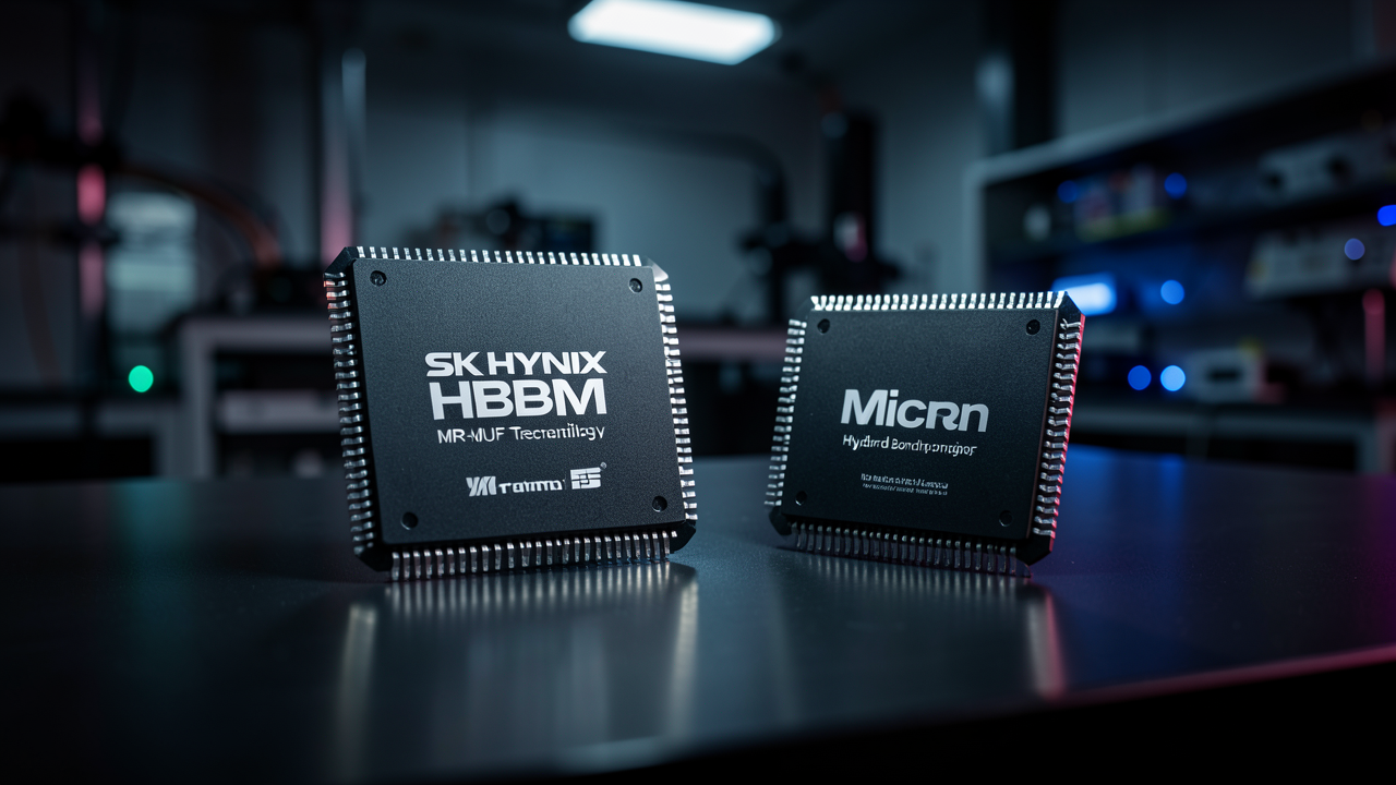
SK Hynix has secured a significant advantage in HBM chip stacking by pioneering ‘Mass Reflow Underfill Molding’ (MR-MUF), a new packaging technology designed to overcome the thermal and physical challenges inherent in HBM die stacking. In parallel, Micron has developed an advanced hybrid bonding technique for stacked chips, which not only reduces thermal resistance at interconnection points but also achieves a remarkable 30% reduction in power consumption compared to rival designs. These breakthroughs are set to redefine the capabilities and efficiency of next-generation semiconductor packaging.
Technical / Clinical Details
SK Hynix’s MR-MUF technology fundamentally addresses the thermal stress and physical deformation issues commonly associated with traditional thermo-compression bonding (TCB) and non-conductive film (NCF) methods. By simultaneously filling and curing underfill resin across multiple HBM dies, MR-MUF ensures uniform thermal distribution and stress mitigation, thereby enhancing HBM module reliability and manufacturing yield for high-density stacks. Micron’s hybrid bonding, on the other hand, utilizes direct copper-to-copper bonding, dramatically increasing interconnect density and improving electrical and thermal conductivity over conventional micro-bump connections. This approach substantially lowers thermal resistance across the interconnect layers, leading to more efficient thermal management for the entire chip and a 30% reduction in power consumption. This power efficiency is particularly crucial for power-intensive AI workloads and contributes significantly to system-level energy savings.
Background & Context
The exponential growth of artificial intelligence and high-performance computing applications has fueled an unprecedented demand for High Bandwidth Memory (HBM). However, advancing HBM performance requires ultra-thin dies, increased stacking layers, and robust solutions for thermal management and mechanical integrity—challenges that conventional packaging technologies struggle to meet. The limitations of older methods have created a bottleneck, making innovative material and process technologies like those from SK Hynix and Micron essential. These advancements are key to resolving the emerging semiconductor shortage specific to HBM supply, which is less about fabrication capacity and more about advanced packaging capabilities.
Strategic Significance & Outlook
The adoption of these advanced packaging technologies by industry leaders like SK Hynix and Micron will profoundly influence the future design and deployment of HBM and next-generation semiconductor products. These innovations are expected to accelerate the proliferation of HBM into thermal-constrained applications, including mobile devices and edge AI hardware. Furthermore, these techniques will drive the evolution of chiplet-based heterogeneous integration and 3D IC architectures, potentially reshaping the broader semiconductor industry roadmap. The enhanced manufacturing efficiency and improved reliability offered by MR-MUF and hybrid bonding will also contribute to cost reductions in final products, further accelerating the widespread adoption of AI chips across various sectors.
Source: https://www.csis.org/analysis/beyond-memory-cycle-ai-hbm-and-new-semiconductor-shortage
Get our weekly technology intelligence — free
Receive an infographic that lets you judge at a glance whether each field’s analysis report is worth reading.
Subscribe Free — Weekly Tech Intelligence
By subscribing, you’ll receive Troy-Technical’s weekly technology intelligence newsletter.
- Your email and selected fields are used only to deliver the newsletter.
- We never share your information with third parties.
- You can unsubscribe anytime via the link in each email.
See our Privacy Policy for details.
Takes about a minute · Unsubscribe anytime






Comments