Key Findings
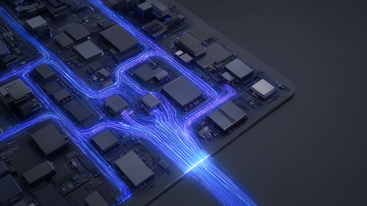
As the semiconductor industry shifts from monolithic Systems-on-Chip (SoCs) to chiplet-based architectures, the Universal Chiplet Interconnect Express (UCIe) 3.0 standard is fundamentally changing how PCI Express (PCIe) is implemented. UCIe 3.0 provides a standardized interconnect optimized for extremely short, high-density, die-to-die communication within a package, significantly contributing to the scalable performance of AI, HPC, storage, and heterogeneous computing systems.
Technical Details
- UCIe 3.0 defines a standardized, high-performance, and low-latency interconnect for chiplets within a package. This allows different chiplets, potentially manufactured on various process nodes or by different vendors, to communicate seamlessly and efficiently.
- A core advantage of UCIe is its ability to decouple process nodes. Computationally intensive chiplets (e.g., CPU cores, AI accelerators) can be manufactured using the most advanced and expensive process nodes (e.g., 3nm, 2nm), while peripheral chiplets, such as PCIe controllers and I/O subsystems, can remain on more cost-effective, mature nodes (e.g., 7nm, 5nm). This approach optimizes overall manufacturing cost while maximizing system performance.
- By leveraging the PCIe protocol layer and optimizing the physical layer for chiplet-to-chiplet links, UCIe 3.0 achieves high bandwidth and low latency. This is crucial for data-intensive workloads in AI inference and training, large-scale HPC, and other high-performance applications in data centers and edge devices.
Background and Context
Facing the limits of Moore’s Law and rising manufacturing costs for monolithic SoCs, the semiconductor industry is embracing chiplet architectures. This paradigm shift requires efficient and standardized communication between chiplets to realize its full potential. Standards like UCIe are central to enabling this successful transition, providing a common language for chiplet interoperability.
Strategic Significance and Outlook
The integration of PCIe with chiplets via UCIe 3.0 has the potential to revolutionize the design and manufacturing of next-generation high-performance computing systems. This technology empowers semiconductor manufacturers to select the optimal process node for specific functionalities, paving the way for more customized, cost-effective, and high-performance chips. Consequently, it will further accelerate the proliferation of AI and the advancement of HPC, opening up new applications and business opportunities across various industries.
Get our weekly technology intelligence — free
Receive an infographic that lets you judge at a glance whether each field’s analysis report is worth reading.
Subscribe Free — Weekly Tech Intelligence
By subscribing, you’ll receive Troy-Technical’s weekly technology intelligence newsletter.
- Your email and selected fields are used only to deliver the newsletter.
- We never share your information with third parties.
- You can unsubscribe anytime via the link in each email.
See our Privacy Policy for details.
Takes about a minute · Unsubscribe anytime








Comments