


Key Findings
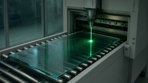
CIT has developed a semiconductor packaging substrate manufacturing solution called ASEDep. This technology is designed to break through the limitations associated with conventional copper used in AI semiconductor packaging by implementing a single-crystal copper deposition process.
Technical Details
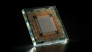
The ASEDep solution utilizes ASE technology to bond copper and insulators into a single-crystal structure. This process enables the production of the CuFlat-PKGCore, a copper flat package core specifically designed for AI semiconductor packages. According to the technical specifications provided, the copper in these cores is deposited to an ultra-flat and ultra-thin state, addressing the physical constraints of traditional packaging materials.
Background and Context
The development of ASEDep addresses the increasing demands of AI semiconductor packaging, where conventional copper deposition methods have faced limitations. To support the production of these substrates, CIT has established a single-crystal copper substrate production facility. The company’s efforts in this field have recently gained recognition, as CIT won the Grand Prize at FLY ASIA, providing the company a platform to showcase its technology in Silicon Valley.
Significance and Outlook
By transitioning from conventional copper to a single-crystal structure, CIT’s ASEDep provides a pathway toward thinner and flatter package cores. This advancement is critical for the scaling and performance requirements of next-generation AI semiconductor packaging, where substrate flatness and material properties directly impact the efficiency of the final package. The integration of the CuFlat-PKGCore into AI hardware represents a shift toward higher precision in substrate manufacturing.
Source: https://www.donga.com/en/article/all/20261015/6420046/1
Get our weekly technology intelligence — free
Receive an infographic that lets you judge at a glance whether each field’s analysis report is worth reading.
Subscribe Free — Weekly Tech Intelligence
By subscribing, you’ll receive Troy-Technical’s weekly technology intelligence newsletter.
- Your email and selected fields are used only to deliver the newsletter.
- We never share your information with third parties.
- You can unsubscribe anytime via the link in each email.
See our Privacy Policy for details.
Takes about a minute · Unsubscribe anytime