

Key Findings
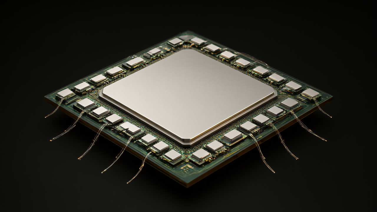
At SEMICON West 2026, NVIDIA presented a prototype chip utilizing Optics-on-Interposer (OOI) technology. This approach moves the Optical Engine (OE) from traditional organic substrates to the silicon interposer, aiming to increase bandwidth density and reduce power consumption for large-scale AI calculations.
Technical Details
The OOI architecture restricts electrical signal transmission within the silicon interposer, utilizing shorter and denser interconnects. This design mirrors the proximity used in current GPU and High Bandwidth Memory (HBM) packaging. NVIDIA provided a comparison using a 200T ASIC package: traditional organic substrate solutions require a component range of 100 mm, whereas OOI concentrates critical components within an 8 mm silicon interposer structure.
Additionally, NVIDIA demonstrated research into dense wavelength-division multiplexing (DWDM). The demonstration utilized 8 optical wavelengths, each operating at 32 Gb/s, achieving a total transmission bandwidth of 256 Gb/s per single optical fiber path.
To mitigate transmission bottlenecks during AI system expansion, NVIDIA integrated microbump technology and low-capacitance interfaces between GPUs and switches.
Background and Context
The OOI technology is the physical realization of theories proposed by NVIDIA Chief Research Scientist Nikola Nedovic in a 2023 paper titled “Beyond CPO: Motivations and Methods for Bringing Optics into the Silicon Interposer.” NVIDIA is currently advancing its CPO-related product lineup, which includes BlueField-5, NVLink 8 CPO, Spectrum 7 204T CPO, and CX10.
Significance and Outlook
NVIDIA plans to implement these advancements in the Rosa Feynman solution scheduled for 2028. The Feynman architecture GPU is expected to further integrate CPO optical technology, surpassing the current Rubin Ultra architecture to provide the high-speed transmission foundation required for giant AI computing centers after 2028.
Get our weekly technology intelligence — free
Receive an infographic that lets you judge at a glance whether each field’s analysis report is worth reading.
Subscribe Free — Weekly Tech Intelligence
By subscribing, you’ll receive Troy-Technical’s weekly technology intelligence newsletter.
- Your email and selected fields are used only to deliver the newsletter.
- We never share your information with third parties.
- You can unsubscribe anytime via the link in each email.
See our Privacy Policy for details.
Takes about a minute · Unsubscribe anytime