Key Findings
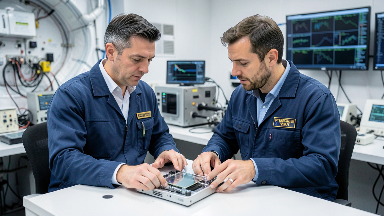
EV Group (EVG) is actively tackling the critical manufacturing challenges inherent in Co-packaged Optics (CPO), a technology poised to revolutionize next-generation interconnects in AI data centers. EVG’s comprehensive portfolio, encompassing wafer bonding, nanoimprint lithography, and thin-wafer processing technologies, supports the essential processes required for high-density integration of Photonic Integrated Circuits (PICs), lasers, and various optical structures within a single package. This significantly paves the way for the mass production and widespread adoption of CPO solutions.
Technical / Clinical Details
CPO technology aims to drastically shorten electrical trace lengths, improve signal integrity, and reduce power consumption and latency by directly integrating optical transceivers into the processor package. EVG’s technologies are indispensable for realizing such complex integration. Specifically, its wafer bonding solutions enable the precise alignment and attachment of dissimilar materials and devices, facilitating heterogeneous integration of silicon photonics with CMOS electronics and III-V semiconductor lasers. Nanoimprint lithography is utilized for manufacturing intricate optical structures and waveguides with high precision and throughput. Furthermore, thin-wafer processing technologies are crucial for minimizing the overall CPO package footprint and optimizing thermal management. Beyond immediate CPO implementation, EVG is also preparing to support future chiplet-based optical I/O architectures and 3D photonic-electronic integration, aiming for an even tighter co-integration of silicon photonics, CMOS, and laser sources.
Background & Context
The explosive growth of AI workloads has intensified the demands on bandwidth and power efficiency for interconnects within data centers. Traditional pluggable optical transceivers are increasingly struggling to scale, and CPO is expected to overcome these limitations, serving as a key enabler for the future of AI computing. However, manufacturing such advanced integrated technologies like CPO presents unprecedented process complexities, particularly concerning precision and yield when integrating diverse materials and functionalities. EVG’s solutions play a central role in mitigating these manufacturing hurdles, thereby accelerating the practical realization of CPO.
Strategic Significance & Outlook
EVG’s advanced manufacturing technologies are set to accelerate the commercialization of CPO, leading to substantial improvements in the performance and power efficiency of AI data centers. The widespread adoption of CPO will fundamentally alter data center design philosophies, enabling GPUs and AI accelerators to operate at their peak performance. In the long term, EVG’s technologies are poised to contribute to the standardization of optical I/O within the chiplet ecosystem and the realization of high-density 3D integration, further deepening the convergence of computing and communication. This progress is expected to powerfully propel the development of next-generation technologies not only in AI but also in HPC, autonomous driving, and IoT.
Get our weekly technology intelligence — free
Receive an infographic that lets you judge at a glance whether each field’s analysis report is worth reading.
Subscribe Free — Weekly Tech Intelligence
By subscribing, you’ll receive Troy-Technical’s weekly technology intelligence newsletter.
- Your email and selected fields are used only to deliver the newsletter.
- We never share your information with third parties.
- You can unsubscribe anytime via the link in each email.
See our Privacy Policy for details.
Takes about a minute · Unsubscribe anytime






Comments