


Key Findings
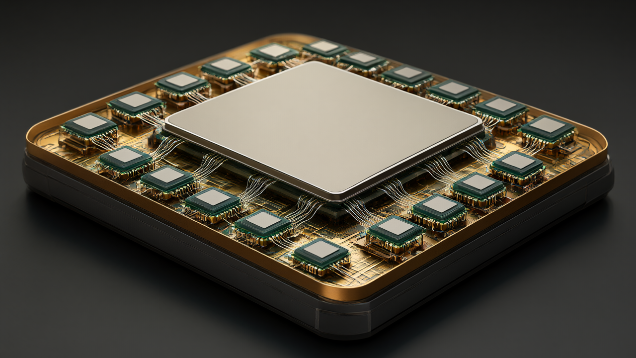
Nvidia is advancing its Co-Packaged Optics (CPO) strategy by introducing Optics-on-Interposer (OOI), a technology that integrates optical engines directly onto the silicon interposer shared with the computing chip. While OOI remains in the research phase, Nvidia is simultaneously scaling existing CPO production, partnering with SPIL to increase CPO optical engine capacity 15-fold by mid-2027 and doubling it again by the end of 2028.
Technical Details
OOI differs from current CPO solutions by bypassing the organic packaging substrate, shortening the electrical signal path between the chip and the optical engine. This design mirrors the logic of HBM connectivity. Additionally, Nvidia is researching Dense Wavelength Division Multiplexing (DWDM) to achieve a total bandwidth of 256Gb/s using eight different wavelengths in a single fiber.
The company’s Spectrum-X Ethernet Photonics switches for the Vera Rubin platform have entered mass production. These systems provide 512 ports of 800Gb/s, totaling 409.6Tb/s of switching bandwidth. According to Nvidia, CPO reduces the power consumption of each 1.6Tb/s port to approximately one-fifth compared to traditional pluggable solutions.
Background and Context
The shift toward OOI is driven by the physical limitations of electrical interconnects. As single-channel rates reach 200Gb/s, signal loss across circuit boards and connectors increases, requiring higher power for equalization and driving circuits. To mitigate this, Nvidia is exploring “wider, slower” parallel interfaces on silicon interposers to reduce complexity and energy consumption.
Significance and Outlook
Integrating optical engines closer to the chip introduces significant engineering challenges, specifically thermal management for temperature-sensitive optical components and increased maintenance costs since integrated engines cannot be replaced as easily as pluggable modules. Testing efficiency is also a bottleneck; TrendForce notes that testing a photonic integrated circuit (PIC) can take over 100 seconds.
This evolution is reshaping the supply chain. Nvidia’s current ecosystem includes TSMC for silicon photonics and COUPE technology, SPIL for packaging and testing, Lumentum and Coherent for external laser sources, and Foxconn for system integration.
Source: https://finance.sina.com.cn/tech/roll/2026-11-01/doc-inixfrfw7836335.shtml
Get our weekly technology intelligence — free
Receive an infographic that lets you judge at a glance whether each field’s analysis report is worth reading.
Subscribe Free — Weekly Tech Intelligence
By subscribing, you’ll receive Troy-Technical’s weekly technology intelligence newsletter.
- Your email and selected fields are used only to deliver the newsletter.
- We never share your information with third parties.
- You can unsubscribe anytime via the link in each email.
See our Privacy Policy for details.
Takes about a minute · Unsubscribe anytime