Background
Perovskite/silicon tandem solar cells are garnering significant attention as a technology capable of surpassing the efficiency limits of current silicon solar cells, with the potential to achieve over 30% power conversion efficiency. To realize this tandem structure, it is crucial to manufacture high-quality, large-area wide-bandgap perovskites (typically around 1.7 eV) to serve as top cells. While solution processes like inkjet printing (IJP) are appealing for their cost reduction potential and scalability, controlling film uniformity and crystal quality, especially crystal orientation, has been a persistent challenge, hindering the achievement of high efficiencies.
Key Findings
This research reports a pioneering method for precisely controlling the crystal orientation of wide-bandgap perovskites through a quenching step within an inkjet printing (IJP) process. This breakthrough enabled perovskite solar cells with a 1.69 eV bandgap to achieve over 20% power conversion efficiency, proving ideal for integration into silicon-perovskite tandem cells as a high-performance top layer.
Technical Details
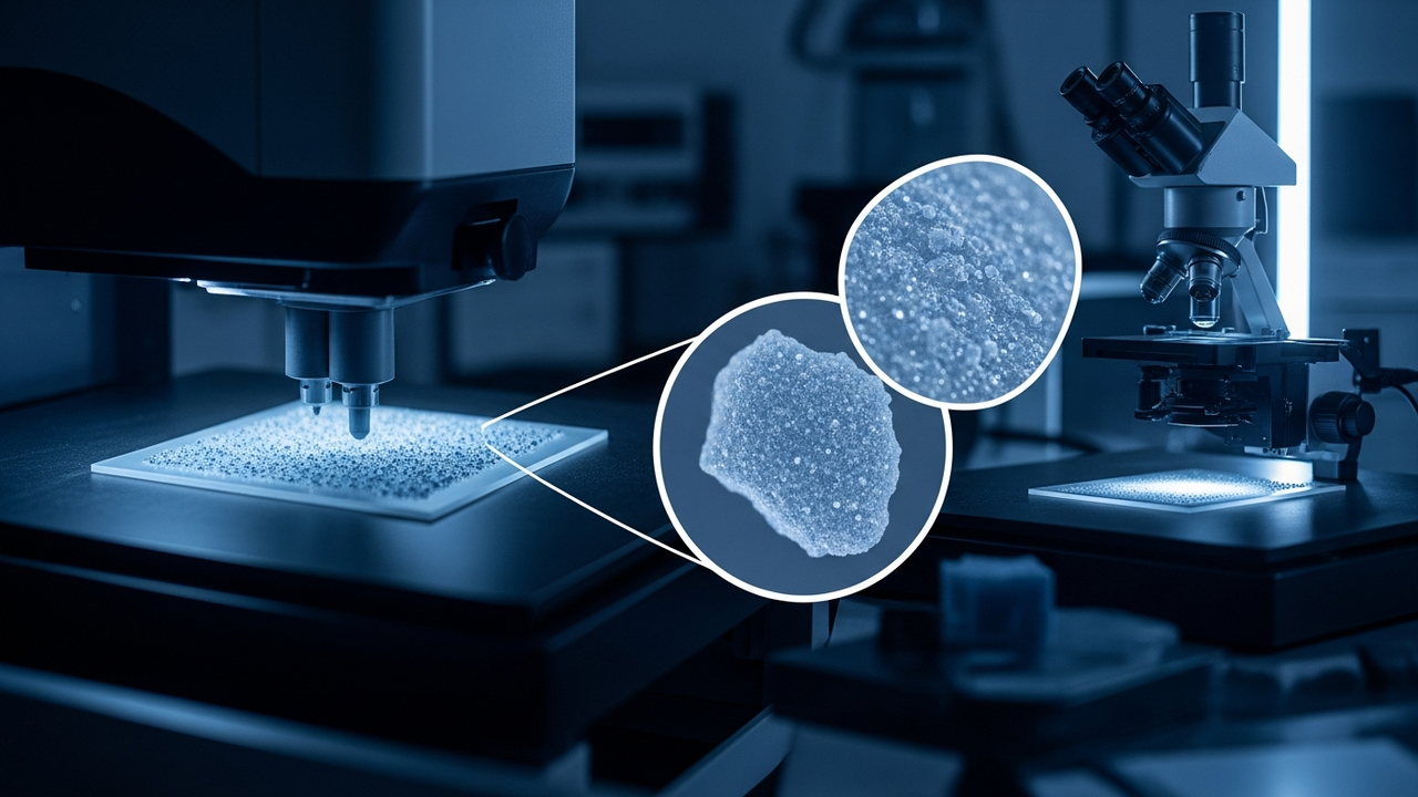
The research team successfully deposited approximately 700 nm thick perovskite films using IJP under controlled ambient air conditions with 55% relative humidity. In this innovative process, the quenching step was found to significantly influence crystal growth dynamics, facilitating the formation of self-assembled monolayer (SAM)-containing wide-bandgap perovskite films with a uniform (110) crystal orientation. This specific crystal orientation is critical as it optimizes charge carrier mobility and lifetime, thereby maximizing the device’s photoelectric conversion efficiency. A 1.69 eV bandgap is an ideal range for efficient utilization of the solar spectrum when combined with a silicon bottom cell, indicating high potential as a high-performing top cell in tandem structures.
Strategic Significance and Outlook
The development of quenching-controlled crystal orientation technology for inkjet-printed wide-bandgap perovskites represents a significant breakthrough for low-cost, large-scale manufacturing of perovskite solar cells. The resulting 1.69 eV bandgap perovskite layer with over 20% efficiency will accelerate the commercialization of perovskite/silicon tandem solar cells as top cells. Moving forward, the research team is expected to further optimize this IJP process, focus on manufacturing large-area devices, evaluating long-term stability, and further reducing manufacturing costs. If successfully introduced to the market, this technology has the potential to dramatically improve the cost-efficiency of solar power and significantly contribute to the widespread adoption of renewable energy globally.
Source: https://pubs.acs.org/doi/10.1021/acsenergylett.6c01417
Get our weekly technology intelligence — free
Receive an infographic that lets you judge at a glance whether each field’s analysis report is worth reading.
Subscribe Free — Weekly Tech Intelligence
By subscribing, you’ll receive Troy-Technical’s weekly technology intelligence newsletter.
- Your email and selected fields are used only to deliver the newsletter.
- We never share your information with third parties.
- You can unsubscribe anytime via the link in each email.
See our Privacy Policy for details.
Takes about a minute · Unsubscribe anytime









Comments