New Technology– category –
-

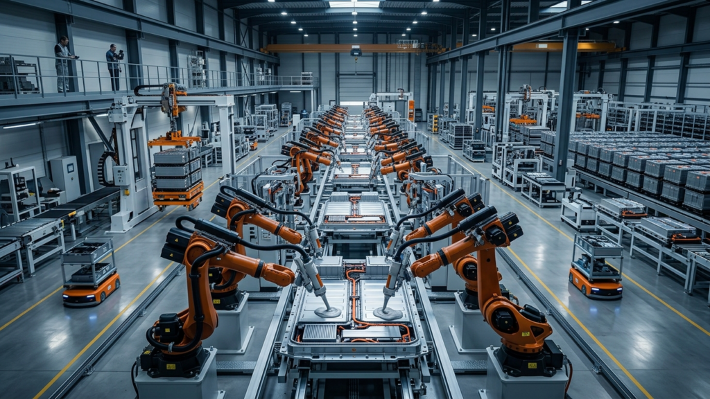
TESA Revolutionizes Car Design and Assembly with Advanced Automotive Adhesives for EV Electrification and HMI Evolution
TESA Germany Overview TESA's advanced automotive adhesive solutions are crucial for the evolving car design and assembly, especially with the shift towards electric vehicles (EVs) and sophisticated human-machine interfaces (HMI). Their c... -
Taiyo Holdings Launches Next-Gen Semiconductor Packaging Material ‘FPIM Series,’ First to Achieve 700nm CD Three-Layer RDL on 12-inch Wafers
PR Newswire Japan Overview Taiyo Holdings, in collaboration with imec, has launched its "FPIM Series," a next-generation semiconductor packaging material that enables the first successful formation of a three-layer Redistribution Layer (... -
Global Battery Manufacturing Reaches 4 TWh as Adhesives for EV Battery Pack Integration Gain Critical Industrial Relevance
24ChemicalResearch Unknown Overview As global battery manufacturing reaches 4 terawatt-hours (TWh), adhesives for EV battery pack integration are gaining critical industrial relevance, driven by the shift towards cell-to-pack (CTP) archi... -
POSTECH Develops Heat-Releasable Medical Patch with Shape-Memory Pyramid Structure, Minimizing Skin Damage for Fragile Skin
CHOSUNBIZ South Korea Overview A research team from Pohang University of Science and Technology (POSTECH), in collaboration with Texas Tech and Northwestern Universities, has developed a medical adhesive patch with adjustable adhesion, s... -
KAIST Develops Glucose-Derived Bio-Hot-Melt Adhesive from E. coli, Outperforming Petroleum Counterparts on Stainless Steel
EurekAlert! Science News South Korea Overview Researchers at KAIST have engineered E. coli to produce novel bio-based hot-melt adhesive polymers (poly(4HB-co-PhLA) and poly(3HB-co-4HB-co-PhLA)) from glucose, presenting a sustainable alte... -
Semiconductor Equipment & Materials Market for HBM, Chiplets, and Low-CTE Materials Forecasted to Outpace Overall Wafer Equipment Growth
Mobility Foresights India Overview A Mobility Foresights report projects that the semiconductor equipment and materials market supporting sub-3nm logic, HBM, and chiplet integration will grow faster than the overall wafer equipment marke... -
Semiconductor Progress Bottleneck Shifts from Circuit Design to New Material Integration and Interfacial Control
Astra Trainer USA Overview Astra Trainer reports that the primary constraint on semiconductor advancement has shifted from circuit design to the integration of novel materials. Device failures often occur at interfaces, not within bulk m... -
Panel Warpage Control Emerges as Key Bottleneck Hindering FOPLP Cost Advantage in Advanced Packaging
EAA Partners - Substack USA Overview Panel warpage control is identified as a critical bottleneck preventing Fan-Out Panel Level Packaging (FOPLP) from realizing its theoretical cost advantages in advanced semiconductor manufacturing. Th... -
Sub-2nm Nodes Blur Process Boundaries as Chiplet Integration Drives Increased Thermal Density and Structural Stress, Hybrid Bonding Emerges as Key Solution
Semiconductor Engineering USA Overview At sub-2nm process nodes, shrinking transistors and heightened process sensitivities are blurring traditional manufacturing boundaries, leading to increased thermal density and structural stress in ... -
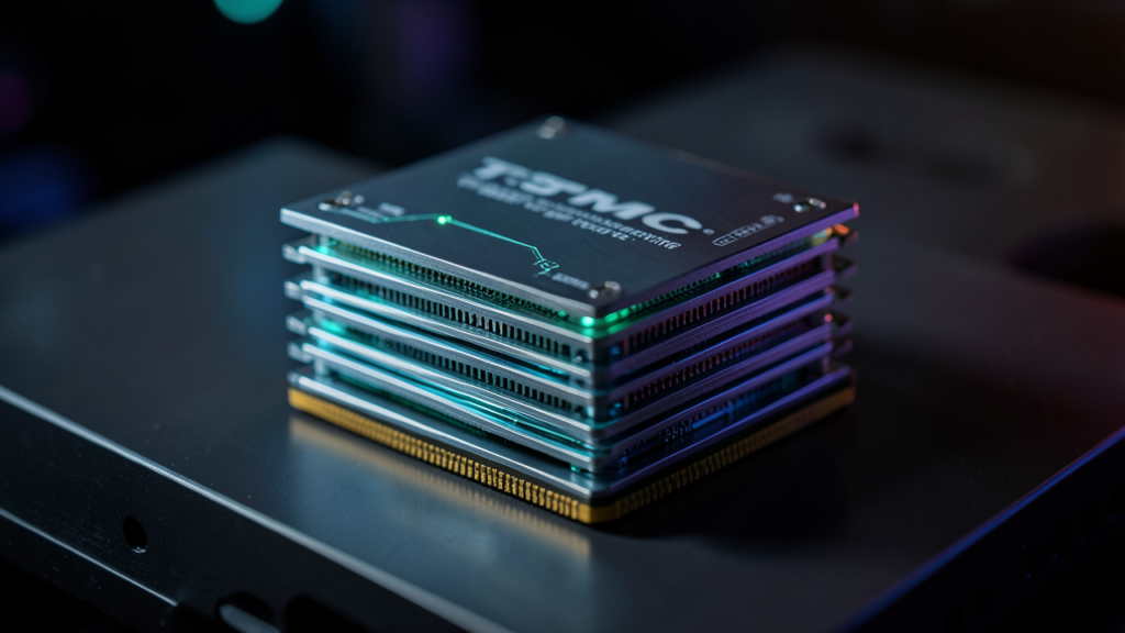
Advanced AI Chips Face Intensified Thermal Management Challenges: TSMC Plans 20-Layer HBM Integration in 14x Reticle CoWoS by 2028, Microchannel Cooling Emerges as Key Technology
36Kr China Overview Thermal management has become a critical challenge in advanced-packaged AI chips, particularly due to thermal coupling issues across chiplets in 2.5D, 3D IC, CoWoS, and HBM architectures. TSMC's roadmap for 2028 inclu...