EDA– tag –
-

Rapidus and Cadence Partner on Agentic AI for Advanced SoC Design, Driving System-Level Co-Optimization
Las Vegas Sun USA Overview Japan's Rapidus announced a partnership with Cadence to drive system-level co-optimization for Agentic AI-enabled advanced SoC (System-on-Chip) design. This collaboration emphasizes tight integration across sem... -
Cadence and Samsung Foundry Deepen 2nm and 3D-IC Collaboration to Meet Surging AI Infrastructure Demand
Chiplet News USA Overview Cadence and Samsung Foundry are deepening their collaboration in 2nm process technology and 3D-IC (3D Stacked Integrated Circuit) technology to address the surging demand for AI infrastructure and physical AI. T... -
Synopsys Enhances Power and Performance for AI and Multi-Die Designs on Latest Samsung Foundry Processes
Chiplet News USA Overview Synopsys announced solutions at SAFE Forum 2026 to enhance power efficiency and performance for AI and multi-die designs, leveraging Samsung Foundry’s latest process technologies. This initiative directly addres... -
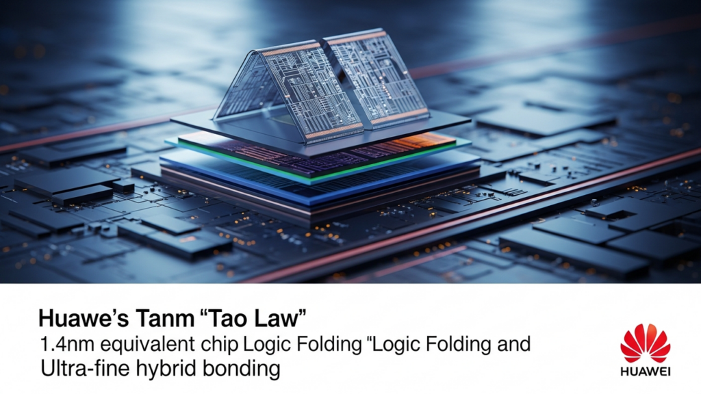
Huawei’s “Tao Law” Proposes 1.4nm-Equivalent Chip Density via Logic Folding and Ultra-Fine Hybrid Bonding
China as a System China Overview Huawei has introduced the "Tao Law," a novel semiconductor process development aiming for 1.4nm-equivalent chip density within five years through "Logic Folding." This method distributes logic gates acros...

1