Samsung Electronics– tag –
-

Samsung Electronics Advances “2.xD” Packaging Integrating HBM, Logic, and Optical Tech to Resolve AI Power and Heat Bottlenecks
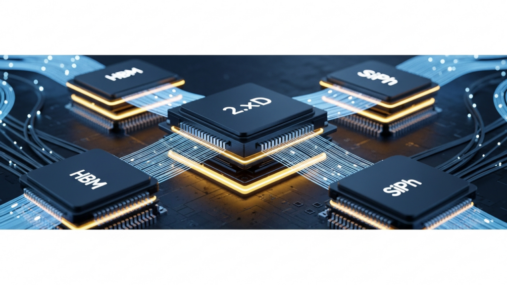
BigGo Finance South Korea Overview Samsung Electronics is developing "2.xD" next-generation packaging technology that integrates High Bandwidth Memory (HBM), logic chips, and silicon photonics (SiPh) into a single package to address crit... -
Taiwan’s TGV Glass Substrate Supply Chain Advances: E&R Engineering Ships Laser Modification Equipment to US Client, Accelerating Mass Production
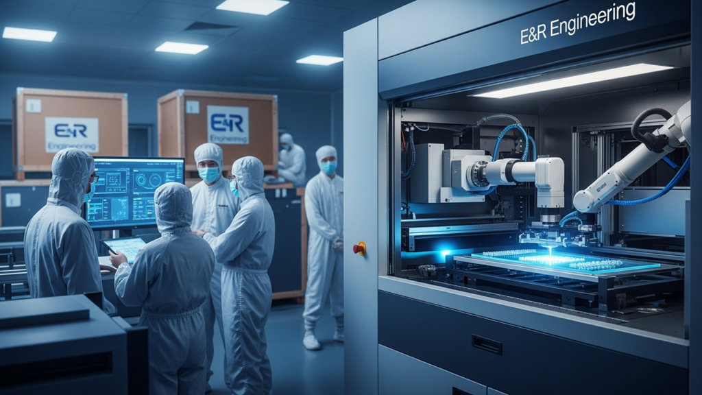
Taiwan News Taiwan Overview Driven by escalating HPC demand, glass substrates are emerging as a next-generation advanced packaging solution, leading to the formation of a robust Through-Glass Via (TGV) supply chain in Taiwan. E&R Eng... -
TSMC’s N3 Node and Expanding CoWoS Capacity Solidify Nvidia’s Future, While HBM4 Multi-Vendor Qualification Reduces Supply Risk
Seeking Alpha USA Overview TSMC and ASML's raised guidance confirms persistent AI infrastructure demand-supply imbalance. TSMC's N3 node, utilized for Nvidia's Rubin GPUs, is fully booked, and CoWoS advanced packaging capacity is expandi... -
TSMC Leads in Data Center Co-Packaged Optics, While Samsung Pursues Future AI Packaging with HBM, Logic, and SiPh Integration in ‘2.xD’ Technology
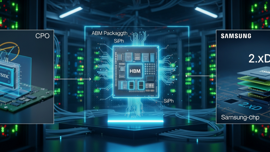
KuCoin International Overview TSMC leads the data center co-packaged optics (CPO) switch market, with Broadcom and NVIDIA already sampling or shipping CPO switches based on TSMC's technology. Concurrently, Samsung is developing '2.xD' ad... -
HBM Supply Crunch Deepens: DRAM Wafer Production and Advanced Packaging/Test Emerge as Dual Bottlenecks Amid Samsung, SK Hynix, Micron Rivalry
Industry Analysis International Overview High Bandwidth Memory (HBM), central to AI, faces dual bottlenecks in both DRAM wafer manufacturing and advanced packaging/test capacity. HBM achieves high bandwidth and energy efficiency through ... -
Samsung Develops ‘2.xD’ Advanced Packaging Integrating HBM, Logic, and SiPh to Tackle AI Data Center Power and Data Bottlenecks
DigiTimes Taiwan Overview Samsung Electronics is developing '2.xD' advanced packaging technology that integrates HBM, logic chips, and silicon photonics (SiPh) into a single package. This innovation aims to resolve critical power consump... -
ASE Initiates Largest-Ever Global Expansion to Double CoWoS Capacity to 45,000 Wafers/Month by Late 2027
Industry Blog/Analysis International Overview ASE is undertaking its largest global factory expansion in history, commencing construction of six new packaging and testing plants in 2026. This aggressive ramp aims to increase monthly CoWo... -
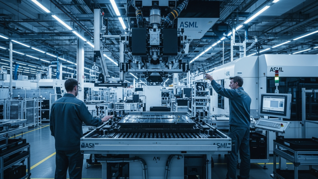
ASML to Increase EUV and DUV Capacity by Nearly One-Third Annually to Alleviate AI Chip Supply Chain Concerns
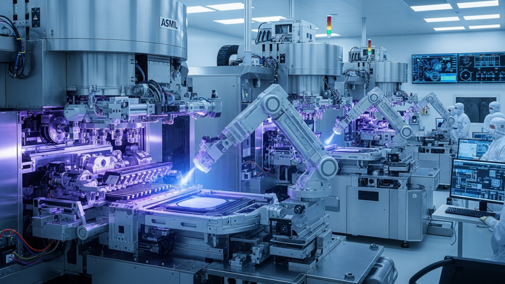
ET Electronics News India Overview ASML, a leading semiconductor equipment supplier, announced an annual production capacity increase of nearly one-third (approximately 33%) for its flagship EUV and DUV tools. This expansion aims to meet... -
ASML Scales Up to Meet AI Chip Demand Surge, Elevates 2026 Outlook
TheFlghts Europe Overview ASML, the dominant provider of lithography equipment, is significantly expanding its production capacity for advanced AI chips in response to unprecedented global demand. The company has consequently raised its ... -
Samsung, SK Hynix, and Micron Invest Billions to Massively Expand AI Chip Memory Production Capacity
The Korea Herald South Korea Overview Major memory semiconductor companies Samsung Electronics, SK Hynix, and Micron Technology are aggressively expanding their production capacity for AI-specific memory chips, including High Bandwidth M...