TSV– tag –
-

Samsung’s Aggressive HBM4 Investment Targets Top HBM Market Share Next Year, Attracting NVIDIA and AMD Interest
Sammy Fans South Korea Overview According to UBS forecasts, Samsung Electronics is poised to become the world's leading HBM memory manufacturer next year, driven by aggressive investments and expanded production in HBM4. The rapid surge ... -
Micron Initiates Mass Production of 36GB 12-Layer HBM4 for NVIDIA Vera Rubin, Boosts US Semiconductor Investment Over $250 Billion
openPR.com USA Overview Micron Technology commenced mass production of its advanced 36GB 12-layer HBM4 memory in March 2026, shipping to NVIDIA for its Vera Rubin platform. This move underscores the market's rapid shift towards higher-ca... -
JEDEC Relaxes HBM4 Package Height to 775 µm, Enabling 12-Hi/16-Hi Stacks Without Immediate Cu-Cu Hybrid Bonding
Exponential Industry USA Overview JEDEC has relaxed the HBM4 package height specification from 720 µm to 775 µm, allowing for 12-Hi and 16-Hi stack HBM modules without immediate reliance on Cu-Cu hybrid bonding. HBM utilizes 3D stacked D... -
TrendForce Analyzes: 18 Chinese Enterprises Accelerate Positions in Glass Core Substrate Market
TrendForce Taiwan Overview TrendForce reported that 18 Chinese companies are rapidly enhancing their presence in the glass core substrate market for advanced packaging. This movement is part of China's strategy to achieve supply chain au... -
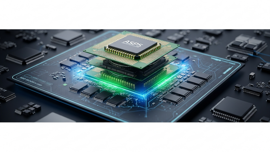
Advanced Semiconductor Packaging & Chiplet Show (ASPS) 2026 in Suwon, Korea, to Cover Advanced Packaging, Chiplets, and HBM
Advanced Semiconductor Packaging & Chiplet Show (ASPS) South Korea Overview The Advanced Semiconductor Packaging & Chiplet Show (ASPS) will take place from August 26-28, 2026, at the Suwon Convention Center in South Korea. This B2B e... -
Intel Accelerates Next-Gen AI Semiconductor Development in U.S. Fabs with Foveros and Enhanced EMIB-T Packaging
Intel USA Overview Intel is aggressively advancing next-generation AI semiconductor development in its U.S. fabs by leveraging cutting-edge advanced packaging technologies such as Foveros stacking, EMIB silicon bridges, and particularly ... -
TSMC and NVIDIA’s ‘Glass Killer’: How Glass Core Substrates Will Revolutionize AI Chips by 2028
SETN Taiwan Overview Renowned analyst Kuo Ming-Chi reveals TSMC's secretive development of 'glass core substrates' in collaboration with NVIDIA, poised to be a game-changer for next-generation AI chip manufacturing. This innovative techn... -
HBM Supply Crunch Deepens: DRAM Wafer Production and Advanced Packaging/Test Emerge as Dual Bottlenecks Amid Samsung, SK Hynix, Micron Rivalry
Industry Analysis International Overview High Bandwidth Memory (HBM), central to AI, faces dual bottlenecks in both DRAM wafer manufacturing and advanced packaging/test capacity. HBM achieves high bandwidth and energy efficiency through ... -
Applied Materials Unveils Seven New Systems for AI Chip DRAM Performance and Advanced 3D Packaging, Accelerating Bottleneck Resolution
Industry News International Overview Applied Materials introduced seven new semiconductor manufacturing systems designed to address bottlenecks in AI chip production, specifically enhancing DRAM performance scaling and advanced 3D packag... -
Micron’s HBM Order Book Fully Committed Through 2028, Secures Silicon Wafer Supply with 10-Year GlobalWafers Offtake Agreement
Investing.com USA Overview Micron Technology's High-Bandwidth Memory (HBM) order book is fully committed through 2026 and 2027, with customer bookings extending into 2028, clearly indicating that supply, not demand, is the binding constr...