Underfill– tag –
-

Mastering 3D-IC Verification Complexity: Multiphysics Analysis Key to Addressing Thermal, Mechanical Stress, and Reliability Challenges
Semiconductor Engineering USA Overview As the semiconductor industry transitions from 2D to 2.5D and 3D-IC configurations, verification complexity is escalating significantly. This article emphasizes the necessity of multiphysics analysi... -
PCIM Europe 2026 Unveils Innovations in Power Module Reliability and SiC/GaN Power Semiconductor Packaging Technologies
MacDermid Alpha, PCIM Europe Germany Overview PCIM Europe 2026 in Nuremberg, Germany, featured significant innovations in power module reliability and next-generation power semiconductor packaging. MacDermid Alpha unveiled underfills, hi... -
Scanning Acoustic Microscopy (SAM) Enables High-Precision Non-Destructive Detection of Internal Defects in Semiconductor Packaging
Infinita Lab USA Overview Scanning Acoustic Microscopy (SAM) is highlighted as a critical non-destructive tool for high-precision evaluation of internal defects in semiconductors, electronic packaging, and material science. SAM excels at... -
NVIDIA Locks Down Multi-Year HBM Supply Deals, Anticipating Persistent Shortages Beyond 2028
gagadget.com USA Overview NVIDIA CEO Jensen Huang recently visited South Korea, securing multi-year agreements with key partners including SK Hynix, SK Telecom, Naver, and Doosan Group for High Bandwidth Memory (HBM) supply, AI cloud inf... -
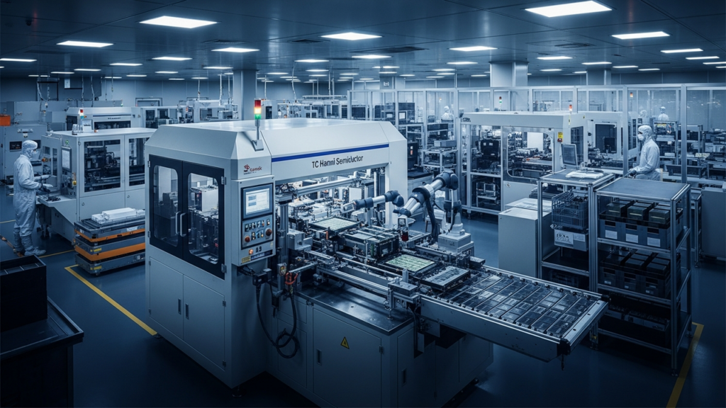
SK Hynix Boosts HBM4 Production with Major TC Bonder Order from Hanmi Semiconductor
The Korea Herald South Korea Overview SK Hynix has made a significant investment, ordering ₩44.2 billion (approx. $28.7 million USD) worth of advanced 'TC Bonder 4.5 Griffin' thermo-compression bonders from Hanmi Semiconductor. This stra... -
Henkel Adhesives Innovates Advanced Semiconductor Packaging Materials for High-Performance Computing and Generative AI
Henkel Adhesives Germany Overview Henkel is developing innovative material solutions for advanced semiconductor packaging, addressing demands for higher performance, greater integration, and improved efficiency in a rapidly evolving tech... -
SemiMedia Reports China Accelerating Global Catch-Up in Advanced Packaging Materials for AI and HPC
SemiMedia China Overview A SemiMedia report indicates that China is accelerating its global catch-up in advanced packaging materials, driven by the demand for AI chips and high-performance computing (HPC). The focus is on developing high... -
JSR Fortifies Advanced Semiconductor Material Production and R&D in Taiwan to Meet Surging AI Demand
JSR株式会社 Japan Overview JSR, a leading semiconductor materials manufacturer, announced a significant expansion of its production and R&D capabilities in Taiwan, effective April 2026. This strategic move, driven by key customer req...