
Key Findings
Researchers have developed an innovative technique called ‘Ion-Beam Origami,’ which enables the fabrication of 3D photonic nanostructures across an entire wafer in just seconds. This groundbreaking manufacturing method achieves over 100 times faster speeds compared to traditional techniques, effectively overcoming the largest barrier to scalability in high-performance 3D optical chip manufacturing. This advancement holds the potential to dramatically accelerate the commercialization and widespread adoption of optical computing technologies.
Technical / Clinical Details
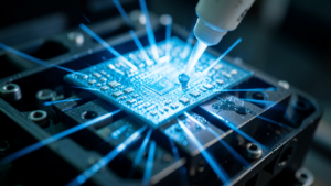
Ion-Beam Origami refers to a process that precisely controls focused ion beams (FIB) to directly create intricate nanoscale structures on materials, subsequently forming 3D architectures through self-assembly. Conventional 3D photonic chip manufacturing relies on multi-stage lithography processes or additive manufacturing techniques, which are both time-consuming and costly. This new technology significantly simplifies these complex steps, enabling the batch fabrication of intricate 3D optical chip structures on a single wafer in an astonishingly short time, ranging from seconds to minutes. By reducing manufacturing costs and substantially expanding production volumes, this breakthrough paves the way for the mass production of optical chips essential for applications like AI accelerators and high-speed communication devices.
Background & Context
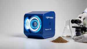
The explosive growth of AI workloads has exacerbated data transfer bottlenecks in data centers and high-performance computing (HPC). Optical computing is anticipated as a next-generation technology to overcome the speed, power consumption, and heat generation limits faced by traditional electronic computing. Major companies like Lightmatter and Intel are actively developing photonic chips for AI workloads, but one of the biggest challenges for their practical implementation has been establishing scalable and cost-effective manufacturing methods. This Ion-Beam Origami technology is of paramount importance in resolving this manufacturing bottleneck and accelerating the industrialization of optical technology.
Strategic Significance & Outlook
The dramatic acceleration of 3D optical chip manufacturing through Ion-Beam Origami will be an indispensable factor in promoting the adoption of optical technology in mainstream computing. This manufacturing breakthrough will enable the mass production of higher-performance, energy-efficient AI accelerators, optical neural networks, and ultra-high-speed optical communication devices. In the future, this technology is expected to accelerate the market introduction of diverse applications built upon optical technology, including quantum computing, AR/VR, and autonomous vehicles. This innovative manufacturing technique will play a crucial role in ushering in a new era of information processing and strengthening the technological foundation for AI to deeply permeate all aspects of society.
Source: https://www.intelligentliving.co/optical-chip-fabrication-hours-seconds/
Get our weekly technology intelligence — free
Receive an infographic that lets you judge at a glance whether each field’s analysis report is worth reading.
Subscribe Free — Weekly Tech Intelligence
By subscribing, you’ll receive Troy-Technical’s weekly technology intelligence newsletter.
- Your email and selected fields are used only to deliver the newsletter.
- We never share your information with third parties.
- You can unsubscribe anytime via the link in each email.
See our Privacy Policy for details.
Takes about a minute · Unsubscribe anytime





Comments