Key Findings
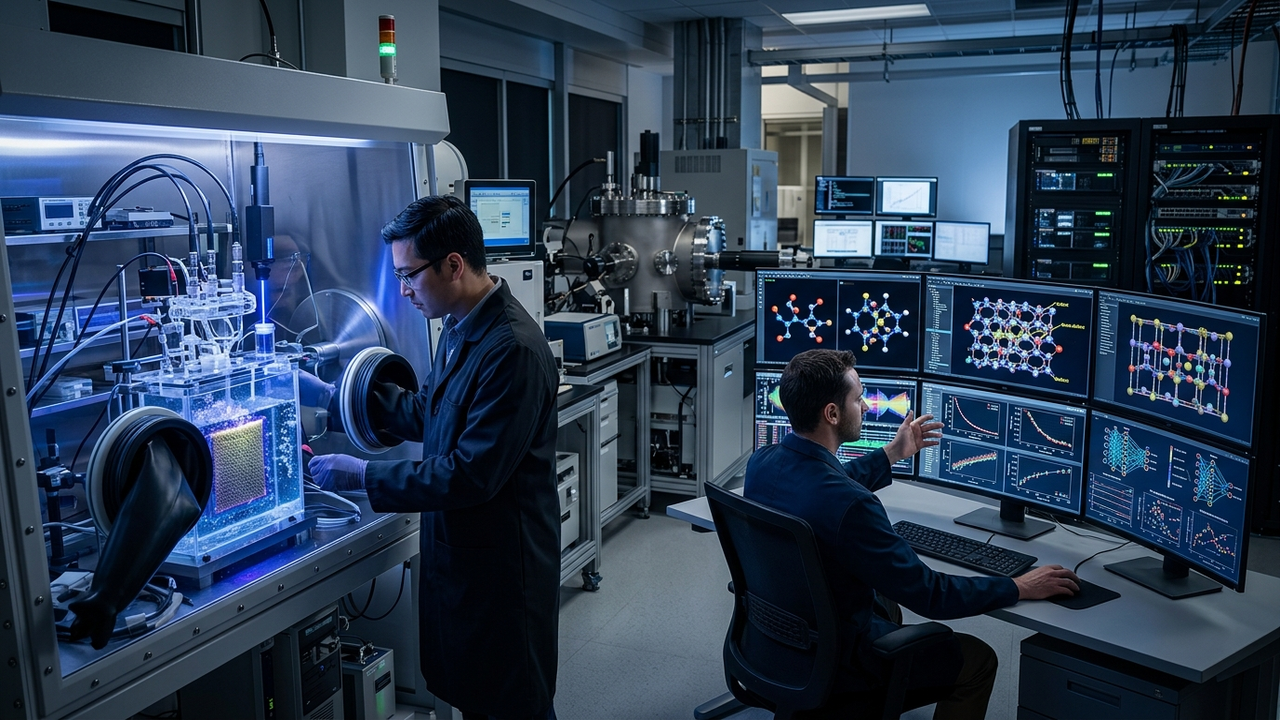
The research team at Lawrence Livermore National Laboratory (LLNL) has achieved a breakthrough in optimizing photoelectrochemical (PEC) devices through the integrated use of ab-initio density functional theory (DFT) simulations with advanced hybrid functionals and computational materials diagnostics. This novel computational capability provides a clear methodology to diagnose the causes of discrepancies between ideal PEC device operation and observed performance. Furthermore, it offers effective procedures for identifying optimal synthesis and processing conditions for individual component materials. By meticulously analyzing the impact of point defects on photoelectron effects and verifying how doping and alloying can optimize critical properties such as electronic conductivity, band gap, light absorption characteristics, and band edge positions, this work holds the potential to dramatically enhance the efficiency and stability of PEC devices.
Technical & Clinical Details
PEC devices hold immense promise for clean energy conversion, such as water splitting using sunlight to produce hydrogen. However, their conversion efficiency and stability largely depend on the properties of the semiconductor materials employed. LLNL’s approach utilizes high-precision hybrid DFT calculations to simulate the subtle atomic-level influences of electronic structures, particularly point defects, on light absorption and charge transport within materials. These simulations quantitatively evaluate how point defects, such as oxygen vacancies or interstitial atoms, affect band gap size, carrier mobility, and photocatalytic activity. Moreover, the research predicts the optimal concentration and form in which specific dopants (e.g., transition metal elements) or alloys (e.g., combinations of different semiconductor materials) should be introduced to maximize the material’s electronic conductivity and achieve appropriate band gap and band edge positions. These computational results serve as direct guidelines for experimental material synthesis, significantly reducing trial-and-error cycles and shortening development times.
Background & Industry Context
Clean energy technologies, particularly solar energy-driven fuel production, are crucial for addressing global energy crises and climate change. PEC devices are one such promising technology, yet existing devices face challenges related to high cost, limited efficiency, and durability. Many of these issues stem from suboptimal design of active layer materials or defect formation during synthesis processes. Computational materials science, especially the combination of DFT simulations with AI, offers a powerful tool to understand atomic-level material behavior and predict performance. LLNL’s research aims to resolve materials design bottlenecks for realizing high-performance PEC devices and contributing to the establishment of a sustainable hydrogen economy.
Strategic Significance & Outlook
LLNL’s computational materials diagnostics and optimization procedures will set new standards for PEC device research. In the future, this approach could evolve into a fully autonomous material discovery and optimization platform when integrated with AI. This will accelerate the design of new catalysts and light-absorbing materials for other clean energy conversion technologies, such as solar water splitting, CO2 reduction, and fuel cells. Furthermore, it is expected to contribute to optimizing defect engineering for improved device stability and longevity, significantly advancing the commercialization of PEC devices. This technology clearly demonstrates how the fusion of computational materials science and AI is a powerful tool for solving critical technological challenges towards achieving a sustainable society.
Get our weekly technology intelligence — free
Receive an infographic that lets you judge at a glance whether each field’s analysis report is worth reading.
Subscribe Free — Weekly Tech Intelligence
By subscribing, you’ll receive Troy-Technical’s weekly technology intelligence newsletter.
- Your email and selected fields are used only to deliver the newsletter.
- We never share your information with third parties.
- You can unsubscribe anytime via the link in each email.
See our Privacy Policy for details.
Takes about a minute · Unsubscribe anytime









Comments