Key Findings
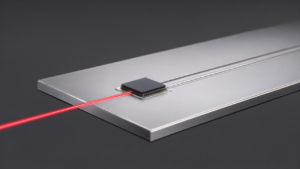
A research team at UC Berkeley has successfully developed a broadband silicon photonics MEMS (Micro-Electro-Mechanical Systems) optical switch using a groundbreaking ‘zero-change foundry-compatible process’ and ‘BEOL (Back-End-of-Line) post-processing.’ They have published a detailed technical paper on this achievement. This novel switch simultaneously achieves a high extinction ratio of over 30dB and an extremely low insertion loss of less than 1.5dB, while exhibiting remarkably low static power consumption of approximately 20nW at maximum actuation voltage, demonstrating exceptional energy efficiency.
Technical / Clinical Details
This MEMS optical switch integrates silicon photonics technology with micromechanics to electrically control the routing of optical signals. Its primary distinguishing feature is the adoption of a ‘zero-change’ approach, which requires minimal modifications to existing semiconductor foundry processes. This enables efficient production while minimizing the need for extensive additional investment in manufacturing facilities. An extinction ratio exceeding 30dB ensures extremely low light leakage during switch ON/OFF states, enhancing signal purity and reliability. Concurrently, an insertion loss below 1.5dB signifies minimal attenuation of optical signals, maintaining signal quality even over long distances or in multi-stage connections. The ultra-low static power consumption of 20nW is particularly beneficial for reducing heat generation and power costs in data centers and edge devices, thereby improving overall system energy efficiency.
Background & Context
AI/ML (Machine Learning) clusters and high-performance data centers demand ultra-fast and efficient transmission of massive data volumes between chips and across racks. Traditional electrical switches have faced challenges related to bandwidth limitations, high power consumption, and heat generation. Optical switches are leading candidates to solve these issues, but manufacturing cost and integration density have been hurdles. UC Berkeley’s research represents a significant step towards practical implementation and widespread adoption of optical switches by enhancing foundry compatibility. Public-private partnerships like AIM Photonics are also driving the industrialization of photonics technology, and this switch holds potential as a foundational component for optical networks in future AI infrastructure.
Strategic Significance & Outlook
This ultra-low-loss, low-power silicon photonics MEMS optical switch has the potential to accelerate the proliferation of optical interconnects in next-generation data centers and AI/ML clusters. Its ability to leverage existing semiconductor manufacturing infrastructure is expected to shorten the path to commercialization. Future efforts will likely focus on further increasing integration density, optimizing dynamic power consumption, and verifying robustness in large-scale network environments. If commercialized, this technology is expected to dramatically enhance AI computing performance and sustainability, enabling more efficient data processing and bringing innovation across a wide range of industries.
Get our weekly technology intelligence — free
Receive an infographic that lets you judge at a glance whether each field’s analysis report is worth reading.
Subscribe Free — Weekly Tech Intelligence
By subscribing, you’ll receive Troy-Technical’s weekly technology intelligence newsletter.
- Your email and selected fields are used only to deliver the newsletter.
- We never share your information with third parties.
- You can unsubscribe anytime via the link in each email.
See our Privacy Policy for details.
Takes about a minute · Unsubscribe anytime