Background
The image sensor market is experiencing exponential growth, propelled by the widespread adoption of smartphones, the proliferation of IoT devices, and rapid advancements in autonomous driving technologies. Crucially, the evolution of artificial intelligence (AI) is transforming sensors from mere image capture devices into intelligent ‘eyes’ capable of sophisticated information analysis and decision-making. In this dynamic environment, optimizing manufacturing processes and enhancing cost-efficiency, alongside boosting intrinsic sensor performance, have become paramount. The alliance between Sony and TSMC, bringing together industry leaders in their respective domains, seeks to comprehensively address these challenges and establish new benchmarks for image sensor technology. This partnership exemplifies a strategic collaboration transcending traditional boundaries of vertical integration and horizontal specialization within the semiconductor industry.
Key Findings
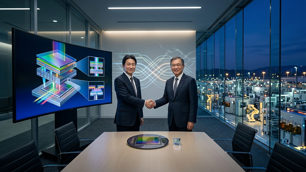
Sony Semiconductor Solutions and Taiwan Semiconductor Manufacturing Company (TSMC), the world’s largest dedicated independent semiconductor foundry, have formalized an agreement to establish a joint venture focused on next-generation image sensors. This landmark partnership is poised to significantly accelerate innovation in image sensor technology, delivering high-performance, feature-rich sensor solutions to the global market.
Technical Details
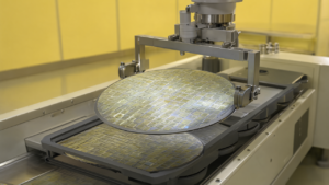
The joint venture will leverage Sony’s world-leading image sensor design expertise in conjunction with TSMC’s cutting-edge process manufacturing capabilities to push the absolute boundaries of sensor performance. Specifically, joint efforts will concentrate on developing novel architectural and process technologies designed to achieve higher resolution, improved sensitivity, wider dynamic range, and significantly lower noise levels. This ambitious endeavor is expected to include the development of innovative pixel structures, high-speed readout circuits, and advanced smart sensors integrating on-chip AI processing capabilities. On the manufacturing front, harnessing TSMC’s advanced production lines will maximize efficiency and quality, ensuring a stable and reliable supply chain for sophisticated image sensors. This collaboration directly addresses the escalating demand for high-performance imaging solutions required across a broad spectrum of applications, including next-generation mobile devices, professional digital cameras, automotive Advanced Driver-Assistance Systems (ADAS), industrial robotics, and critical security surveillance cameras.
Strategic Significance and Outlook
This joint venture holds the profound potential to significantly reshape the competitive landscape of next-generation image sensor technology. By synergistically combining the complementary expertise and vast resources of both companies, the cycle of technological innovation will accelerate dramatically, leading to the emergence of unprecedented applications and services previously considered unimaginable. In the future, the development of smaller, higher-performance, and more power-efficient sensors is expected to drive transformative innovations across diverse fields such as edge AI devices, advanced wearable technology, and precision medical diagnostic equipment. The collaboration between Sony and TSMC marks a crucial strategic step that will not only advance image sensor technology but also contribute substantially to the broader progression of the global electronics industry.
Source: #
Get our weekly technology intelligence — free
Receive an infographic that lets you judge at a glance whether each field’s analysis report is worth reading.
Subscribe Free — Weekly Tech Intelligence
By subscribing, you’ll receive Troy-Technical’s weekly technology intelligence newsletter.
- Your email and selected fields are used only to deliver the newsletter.
- We never share your information with third parties.
- You can unsubscribe anytime via the link in each email.
See our Privacy Policy for details.
Takes about a minute · Unsubscribe anytime