
Key Findings
JX Metals has integrated its semiconductor sputtering targets and Tatsuta Electric Wire’s conductive pastes into the development of next-generation semiconductor packaging. These materials were utilized within the “Hi-CHIP” (Heterogeneous Integration and Chiplet System Package Alliance) project, an international initiative led by the Industrial Technology Research Institute (ITRI) of Taiwan. The results of this collaboration were presented at the IMPACT 2026 international conference on October 21, 2026.
Technical Details
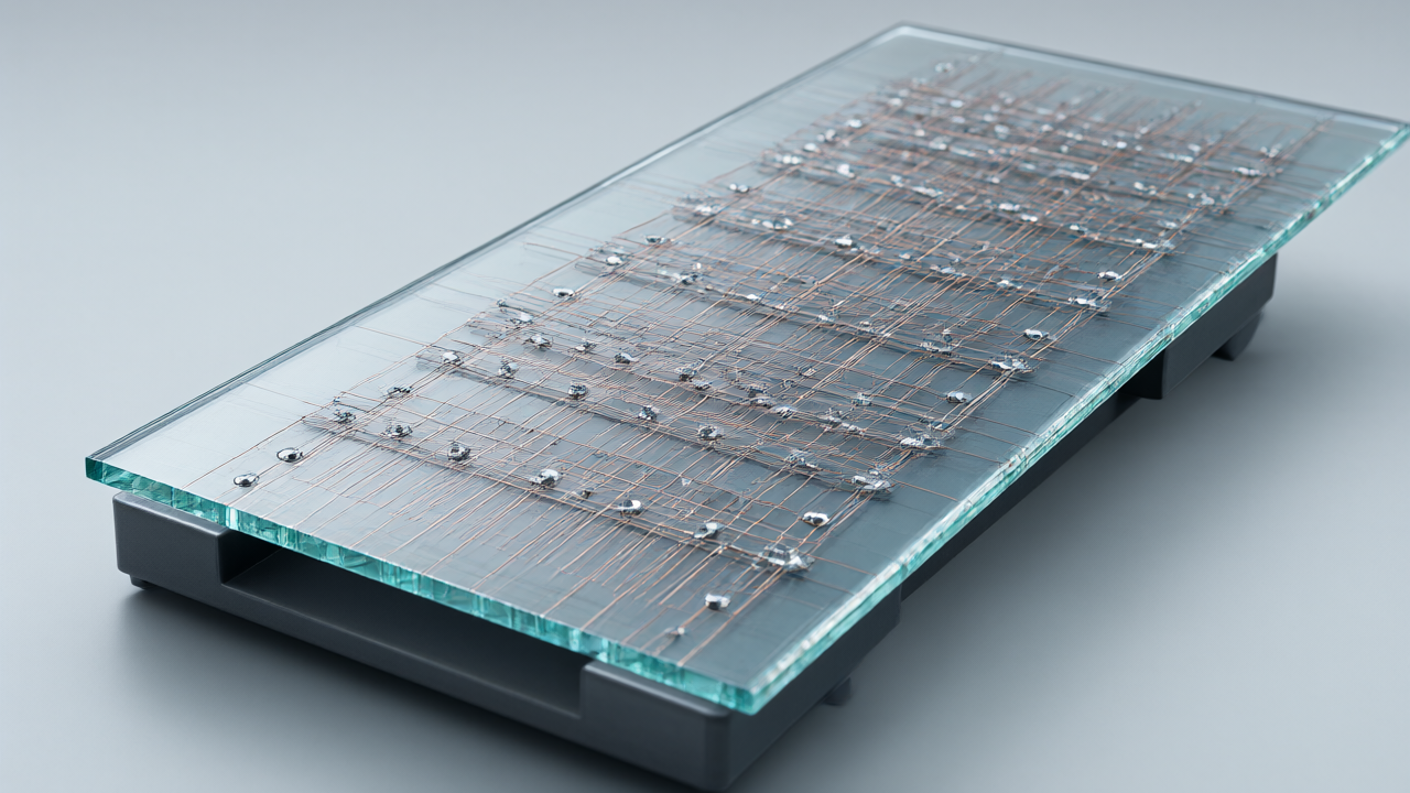
The project focused on two primary glass-based architectures:
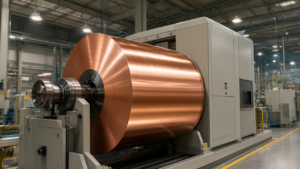
- Glass Interposers: JX Metals’ sputtering targets were used to form the seed layer, which serves as the foundation for creating fine wiring.
- Glass Core Substrates: Conductive paste from Tatsuta Electric Wire was employed to fill Through Glass Vias (TGV), ensuring successful via filling and electrical conductivity.
Glass substrates are preferred for these applications due to their high flatness and dimensional stability. These properties allow for the production of larger substrates while minimizing warping and deformation, enabling the high-precision formation of fine circuitry.
Background & Context
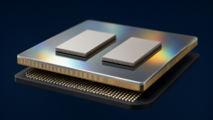
The Hi-CHIP alliance serves as a collaborative platform involving Taiwan-based semiconductor firms—including the Taiwan branches of Intel, ASML Holding, and Applied Materials—alongside international companies specializing in materials, equipment, and assembly. The alliance focuses on the design, prototyping, evaluation, and mass production of advanced packaging for heterogeneous integration and chiplets.
Significance & Outlook
As AI semiconductors require higher performance, the industry is moving toward larger and higher-density packaging. The adoption of glass interposers and glass core substrates is expected to increase the demand for specialized materials, specifically sputtering targets for fine wiring and conductive pastes for via filling. JX Metals intends to support the evolution of these packaging technologies through its material portfolio.
Source: https://monoist.itmedia.co.jp/mn/articles/2611/12/news020.html
Get our weekly technology intelligence — free
Receive an infographic that lets you judge at a glance whether each field’s analysis report is worth reading.
Subscribe Free — Weekly Tech Intelligence
By subscribing, you’ll receive Troy-Technical’s weekly technology intelligence newsletter.
- Your email and selected fields are used only to deliver the newsletter.
- We never share your information with third parties.
- You can unsubscribe anytime via the link in each email.
See our Privacy Policy for details.
Takes about a minute · Unsubscribe anytime