Bonding– tag –
-

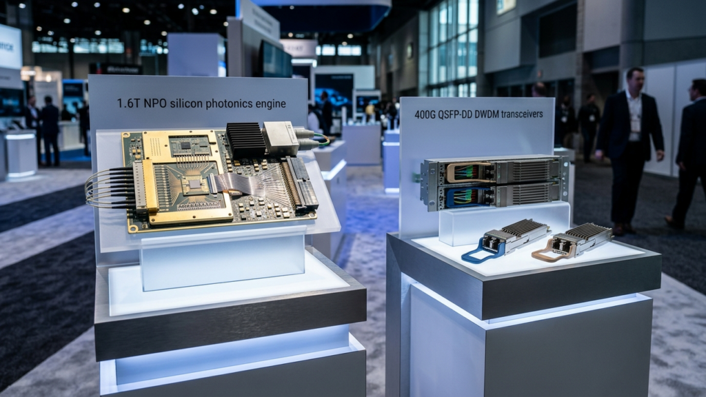
GIGALIGHT Unveils DSP-Free 1.6T NPO Silicon Photonics Engine and 400G QSFP-DD DWDM Solution at China Computing Expo
GIGALIGHT China Overview GIGALIGHT showcased a DSP (Digital Signal Processing)-free 1.6T DR16 NPO (Near-Package Optics) linear silicon photonics engine and a dual-approach 400G QSFP-DD DWDM solution at the China Computing Expo. The 1.6T ... -
Kulicke & Soffa Enhances Thermal Compression Bonding (TCB) Technology for Co-Packaged Optics (CPO) to Boost AI Infrastructure
PR Newswire USA Overview Kulicke & Soffa (K&S) announced it is enhancing its advanced packaging portfolio, including Thermal Compression Bonding (TCB) solutions, for Co-Packaged Optics (CPO) applications to meet soaring AI infras... -
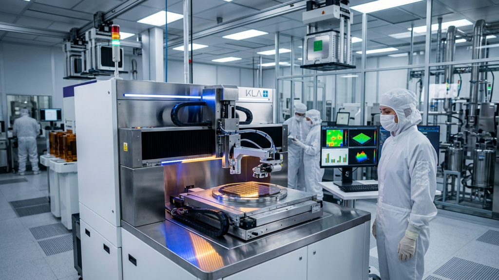
KLA Unveils AI-Powered High-Speed, High-Precision Defect Inspection Solution to Boost Yield in Advanced Packages like CoWoS
SEMI Global USA Overview KLA has introduced a new AI-powered inspection system for high-speed, high-precision defect detection in high-density RDLs and 3D stacked structures. This solution supports yield management in advanced packaging ... -
Applied Materials Unveils New Hybrid Bonding Platform for High-Volume 3D Stacked Chip Manufacturing, Enabling Ultra-Fine Pitch Integration
Business Wire USA Overview Applied Materials has launched a new hybrid bonding platform designed for high-volume manufacturing of next-generation 3D stacked chips. This innovative system achieves high-precision alignment and high through... -
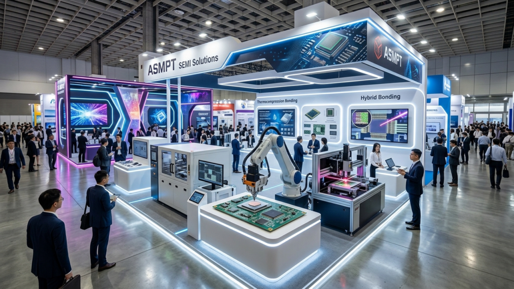
ASMPT to Showcase Advanced Thermocompression and Hybrid Bonding Innovations for HPC and AI at SEMICON Taiwan 2026
ASMPT SEMI Solutions Taiwan Overview Global technology leader ASMPT announced it will showcase its advanced packaging portfolio at SEMICON Taiwan 2026, supporting HPC, AI accelerators, silicon photonics, and Co-Packaged Optics (CPO) appl... -
Rapidus Targets 600mm Panel-Level Packaging and 8-Reticle Interposers by 2030 for Advanced AI/HPC Systems
TrendForce Japan Overview Rapidus announced an accelerated advanced packaging roadmap aiming for 600mm panel-level packaging and 8-reticle interposers by 2030. The company has fully activated its Rapidus Chiplet Solutions (RCS) pilot lin... -
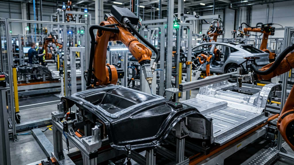
3M Launches Fast-Curing Acrylic Adhesive for Multi-Material Bonding to Lightweight EV Body Structures
3M(3M Automotive Solutions News) USA Overview 3M has announced a new high-strength acrylic adhesive formulated for multi-material bonding in electric vehicle (EV) body structures. This adhesive enables reliable joining of dissimilar ma... -
HANMI Semiconductor Invests $91.4 Million in Largest-Ever 8th Production Facility in Incheon to Meet Soaring AI Chip Demand
Business Wire South Korea Overview HANMI Semiconductor is investing $91.4 million (approximately 130 billion KRW) to establish its largest-ever 8th production facility in Incheon, by acquiring Mercury Co., Ltd.'s factory, to proactively ... -
Semiconductor Inspection Equipment Market to Reach $13.4 Billion by 2034, KLA Leads in Advanced Packaging Process Control
Exponential Industry USA Overview The semiconductor inspection equipment market is projected to grow at a 7.9% CAGR from 2026 to 2034, reaching $13.4 billion, driven by increasing AI chip complexity and advanced packaging adoption. KLA i... -
HBM4 Breaks Bottlenecks: Hybrid Bonding Delivers 20%+ Thermal Reduction, 40% Power Efficiency Boost, 2.0TB/s+ Bandwidth
SemiHub.io International Overview HBM4, the next-generation High Bandwidth Memory, is set to significantly advance AI/HPC performance by doubling its I/O width to 2048 bits, targeting over 2.0 TB/s bandwidth per stack and substantial pow...