Lithography– tag –
-

DNP Develops Nanoimprint Lithography (NIL) Capable of 10x Power Reduction in Semiconductor Manufacturing
DNP Group Japan Overview Dai Nippon Printing (DNP) has developed Nanoimprint Lithography (NIL), a next-generation semiconductor manufacturing technology poised to achieve high-resolution patterning while dramatically cutting power consum... -
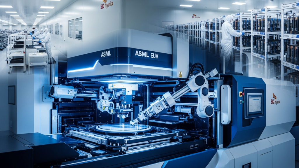
SK Hynix to Heavily Invest in ASML EUV for HBM Production in Yongin and Cheongju, Expanding Indiana Packaging Facility
Seeking Alpha South Korea Overview SK hynix plans to extensively deploy ASML's EUV (Extreme Ultraviolet) lithography equipment at its Yongin Semiconductor Cluster and Cheongju advanced packaging facilities, significantly bolstering High-... -
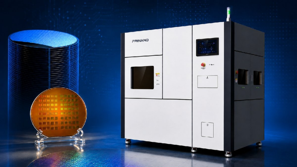
Chinese Startup Prinano Claims Mass Production of 8-inch Photonic Chip Wafers Using Nanoimprint Lithography, Projecting Up to 90% Cost Reduction
New Market Pitch China Overview According to a New Market Pitch analysis, Chinese startup Prinano claims successful mass production of 8-inch photonic chip wafers using nanoimprint lithography (NIL), without conventional DUV lithography.... -
Nanoimprint Lithography Achieves Sub-10nm Resolution with High Throughput and Low Cost for Next-Gen Chip Manufacturing
ChipXpert International Overview Nanoimprint Lithography (NIL) is emerging as a disruptive patterning technology capable of manufacturing sub-10nm feature sizes for future semiconductor chips, offering high resolution, low cost, and high... -
Canon Sets 25% Industrial Unit Profit Margin Target by FY2030, Focusing on Nanoimprint Technology Commercialization
Investing.com Canada (citing Nikkei online) Japan Overview Canon's CFO, Minoru Tanaka, announced a target to increase the operating profit margin of its industrial business to 25% by fiscal year 2030, up from 17.5% in 2026. This ambitiou... -
Prinano’s Nanoimprint Lithography Breakthrough: 8-inch Photonic Chip Production at 1/10th DUV Cost, Challenging Global Incumbents
複数の報道機関 (香港NTI、Semiconductor Engineering、Loano via YouTube) China Overview Chinese startup Prinano Technology has announced the validation of volume production for 8-inch photonic chip wafers using its indigenously developed P... -
Canon Invests ¥50 Billion in New NIL Factory in Japan, Targets 2nm Process to Challenge ASML’s EUV Dominance
Move Silicon Japan Overview Canon is investing ¥50 billion (approximately $320 million USD) in a new lithography equipment factory in Utsunomiya, Japan, to aggressively advance its Nanoimprint Lithography (NIL) technology. The company cl... -
Sub-10nm Residual Distortion Achieved in Low-Distortion Fusion Bonding with Pneumatically Curved Wafers for Advanced Semiconductors
arXiv USA Overview A recent arXiv publication reports the development of a novel low-distortion fusion bonding technique that employs pneumatically curved wafers to achieve an exceptionally low residual grid distortion of less than 10 na... -
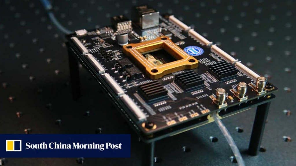
China’s Prinano Achieves Mass Production of 8-inch Photonic Chips with Proprietary Nanoimprint Tech, Bypassing ASML Equipment, Reducing Cost by 10x, and Achieving Sub-10nm Resolution to Circumvent Export Controls
South China Morning Post China Overview Chinese startup Prinano announced successful mass production of photonic chips on 8-inch silicon wafers using its proprietary PL-AS vacuum air-cushion nanoimprint lithography (NIL) equipment, elimi... -
Beyond EUV: Nanoimprint Lithography and Directed Self-Assembly Poised to Redefine Processor Manufacturing
Alibaba.com China Overview While Extreme Ultraviolet (EUV) lithography remains central to advanced processor manufacturing, Nanoimprint Lithography (NIL) and Directed Self-Assembly (DSA) are critical R&D concepts defining future chip...