TSMC– tag –
-

TSMC Narrows CoWoS Supply-Demand Gap from 20% to 10% by End of 2026; NVIDIA to Adopt Next-Gen CoPoS for 2028-2029 Mass Production
Moomoo Singapore Overview TSMC is accelerating advanced packaging capacity expansion, projecting its CoWoS supply-demand gap to significantly narrow from approximately 20% to 10% by the end of 2026. Concurrently, research and development... -
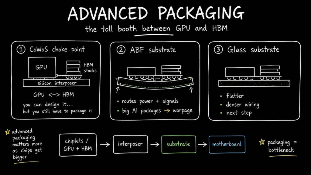
Advanced Packaging: Glass Core Substrates Emerge as Next-Gen Frontier; Intel Commits Over $1 Billion to R&D for High-Volume Production by 2030
Infra Startups USA Overview Advanced packaging is a critical bottleneck in the AI boom, with TSMC's CoWoS capacity dictating the pace of global AI infrastructure build-out. Shipments of CoWoS wafers are projected to reach approximately 4... -
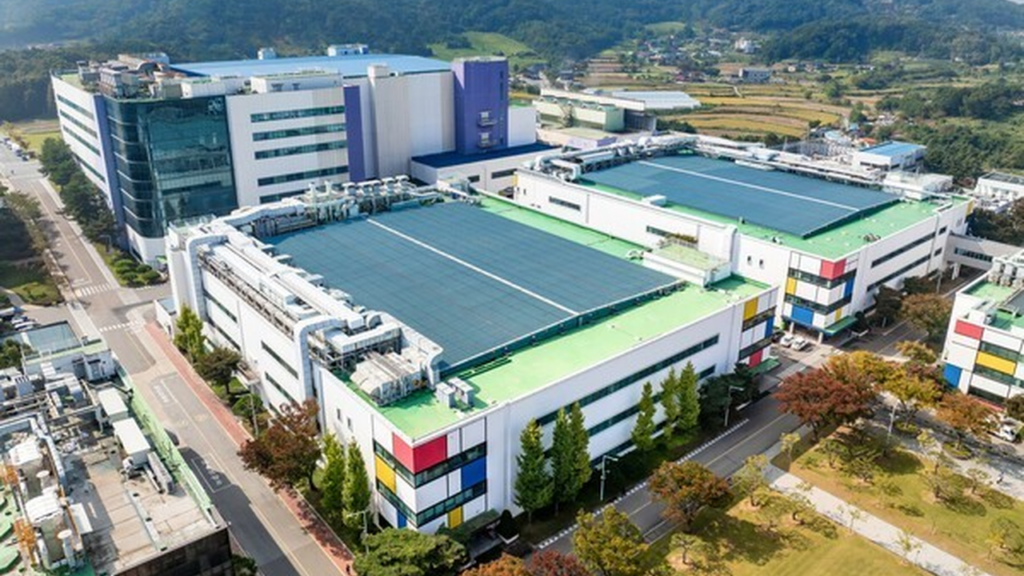
Samsung, SK Hynix Eye Honam Region in South Korea for First Advanced Packaging Fabs Amid Soaring AI Memory Demand; Amkor Plans $980M Expansion
The Elec Inc. South Korea Overview Samsung Electronics and SK Hynix are considering establishing their first advanced semiconductor packaging plants in South Korea's Honam region to meet surging AI infrastructure demand. Samsung is weigh... -
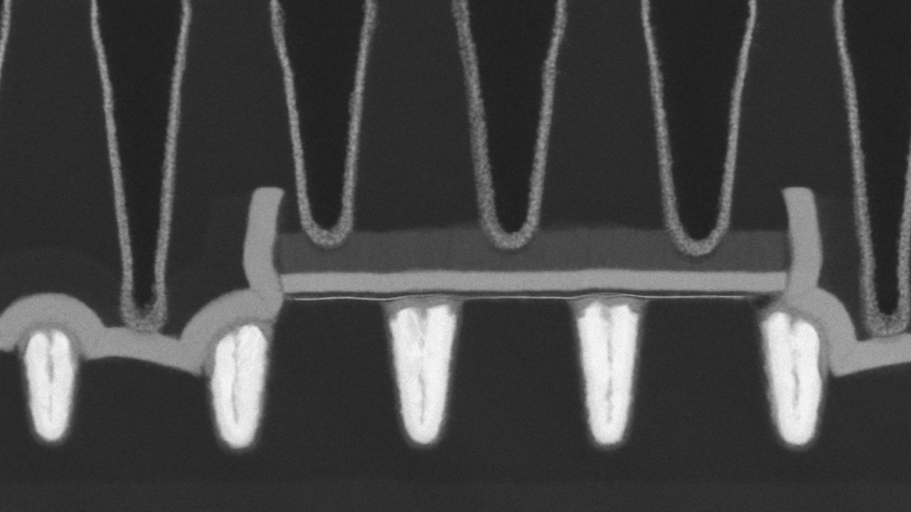
IMEC, ASML, TSMC Scale 2D Material Transistors to 300mm Wafers, Achieving 50nm Contact Poly Pitch for Fab Integration
IMEC ベルギー Overview IMEC, in partnership with ASML and TSMC, has unveiled a robust, scalable 300mm integrated process for n-type and p-type field-effect transistors utilizing 2D materials. Presented at the 2026 IEEE/JSAP VLSI Technolo... -
Tensordyne’s Napier AI Inference System, Taped Out on TSMC 3nm, Achieves 17x More Tokens/Watt and 13x Higher Throughput than NVIDIA Blackwell
Tensordyne USA Overview Tensordyne announced its Napier (TDN) AI inference system, fabricated on TSMC's 3nm process, delivers up to 17x more tokens per watt and 13x higher throughput compared to NVIDIA Blackwell systems. This breakthroug... -
TSMC’s COUPE Platform for Co-Packaged Optics Targets 2026 Mass Production, Integrating Micro LEDs for AI Cluster Performance Boost
The Storm Media Taiwan Overview TSMC has announced the 2026 mass production launch of "COUPE" (Compact Universal Photonic Engine), an innovative platform for co-packaged optics (CPO) interconnects. Utilizing SoIC bonding to stack photoni... -
Apple’s M5 Ultra Pioneers Integration with TSMC’s N3P Process and SoIC-mH Packaging
TrendForce Taiwan Overview Reports indicate Apple's upcoming M5 Ultra chip, expected at WWDC, will likely leverage TSMC's N3P process node and its advanced SoIC-mH (System-on-Integrated-Chips – molded horizontal packaging) technology. So... -
Intel and Tesla Partner on AI6 Data Centers, Tapping Advanced Packaging for Production at Austin’s ‘Terafab’
Jamie's Substack USA Overview Tesla has announced a strategic partnership with Intel Foundry Services to scale its AI6 chip-powered data center clusters, extensively utilizing Intel's advanced packaging technologies. The collaboration wi... -
Advanced Packaging’s Evolution: 2.5D/3D Integration, Chiplets, and Hybrid Bonding Propel AI and HPC
Springer Professional Germany Overview Semiconductor packaging technology has dramatically evolved from 2D to 2.5D and 3D IC integration, a transformation accelerated by the explosive demand from AI and High-Performance Computing (HPC). ... -
Glass Substrates: The Next Frontier in AI Packaging and the Race to Mass Production
The Economy South Korea Overview Glass substrates are rapidly emerging as a transformative technology in advanced AI chip packaging, poised to replace conventional organic substrates and silicon interposers by offering superior dimension...