August 2026– date –
-

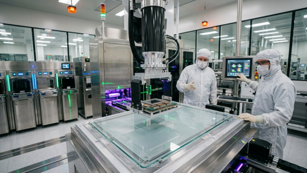
Glass Substrates in Advanced Packaging Accelerate from Prototype to Mass Production, Emerging as Key Technology for HBM and Chiplet Integration
Solid State Technology USA Overview Advanced packaging technology utilizing glass substrates is rapidly transitioning from R&D to mass production within the semiconductor industry. Glass substrates, superior to conventional organic s... -
STMicroelectronics Unveils Modular SiP Solution for Automotive AI Market, Driving Miniaturization and Performance in Autonomous Driving and ADAS
Electronics Weekly Switzerland/France Overview STMicroelectronics has launched a new modular System-in-Package (SiP) solution specifically designed for automotive AI applications. This solution integrates multiple chips to reduce footpri... -
Infineon Strengthens Advanced Packaging Collaboration in Europe under EU Chips Act, Building Chiplet and Heterogeneous Integration Supply Chain
Reuters Germany Overview Infineon announced strengthened partnerships for advanced packaging technology development within Europe, leveraging the EU Chips Act. This strategy aims to build an indigenous supply chain for chiplet technology... -
AT&S Ramps Up HPC Substrate Capacity to Meet Surging Data Center and AI Demand
Business Journal Austria Overview Austrian-based AT&S, a leading package substrate manufacturer, is significantly accelerating its IC substrate capacity expansion, primarily targeting high-performance computing (HPC) applications. Th... -
Fraunhofer IZM Demonstrates High-Density Flexible Hybrid Substrate (FHS) Technology, Opening New Frontiers for Wearable and IoT Devices
Semiconductor Engineering Germany Overview Fraunhofer IZM has demonstrated Flexible Hybrid Substrate (FHS) technology, enabling high-density wiring. This innovative approach integrates diverse semiconductor chips and passive components o... -
imec Pioneers Glass Substrates for Next-Gen 3D Packaging, Accelerating AI/HPC Commercialization
EETimes Belgium Overview imec, the renowned Belgian microelectronics research institute, has announced a significant breakthrough in 3D stacked packaging, leveraging glass substrates as interposers. This innovation is pivotal for next-ge... -
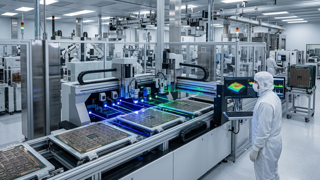
Onto Innovation Unveils High-Precision, High-Speed Metrology Solution to Accelerate Panel Level Packaging Mass Production
Photonics.com USA Overview Onto Innovation has announced a high-precision metrology solution designed to overcome mass production challenges in Panel Level Packaging (PLP). This new technology enables high-speed measurement of fine struc... -
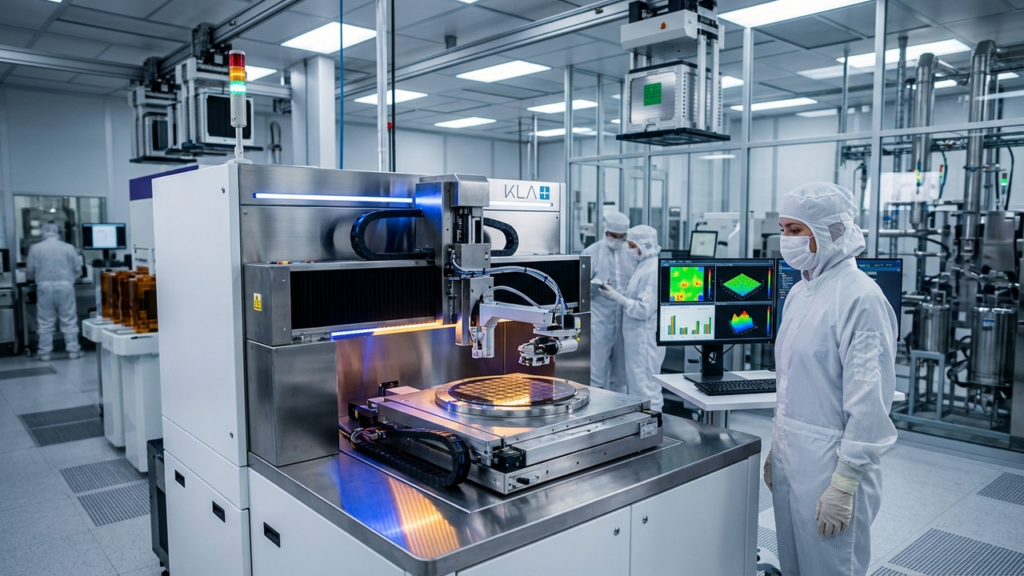
KLA Unveils AI-Powered High-Speed, High-Precision Defect Inspection Solution to Boost Yield in Advanced Packages like CoWoS
SEMI Global USA Overview KLA has introduced a new AI-powered inspection system for high-speed, high-precision defect detection in high-density RDLs and 3D stacked structures. This solution supports yield management in advanced packaging ... -
Applied Materials Unveils New Hybrid Bonding Platform for High-Volume 3D Stacked Chip Manufacturing, Enabling Ultra-Fine Pitch Integration
Business Wire USA Overview Applied Materials has launched a new hybrid bonding platform designed for high-volume manufacturing of next-generation 3D stacked chips. This innovative system achieves high-precision alignment and high through... -
Japan Introduces New Subsidy Program for Advanced Packaging R&D, Focusing on Heterogeneous Integration and 3D Stacking to Enhance Competitiveness
METI Press Release Japan Overview Japan's Ministry of Economy, Trade and Industry (METI) unveiled a new subsidy program to support R&D and mass production investment in advanced packaging technologies for strengthening the domestic s...