
Key Findings
Brewer Science is set to unveil new data at IMAPS 2026 on a high-temperature-stable laser release material, specifically engineered to withstand and perform in advanced semiconductor packaging processes operating at 250°C to 350°C. This breakthrough material addresses a critical need for robust temporary bonding and debonding solutions in high-thermal budget manufacturing environments.
Technical Details
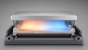
The new laser release material is designed to be compatible with challenging high-temperature processes such such as plasma-enhanced chemical vapor deposition (PECVD), hybrid bonding, silver sintering, and thermocompression bonding. It forms a core component of the Temporary Bond/Debond (TBDB) system. When paired with BrewerBOND® C1301 series adhesives, this system demonstrates exceptional structural integrity even after exposure to process temperatures up to 350°C. Furthermore, it exhibits reliable debonding performance when subjected to 308nm and 355nm UV laser wavelengths. Post-debonding, the material facilitates a straightforward, solvent-based cleanup process, ensuring minimal residue and a pristine surface for subsequent manufacturing steps.
Background & Context
The relentless drive towards higher performance, increased integration, and miniaturization in semiconductor devices, particularly for AI, HPC, and automotive applications, necessitates more sophisticated packaging technologies. These advanced packaging schemes often involve multiple high-temperature processing steps that can degrade conventional temporary bonding materials. The inability of existing materials to maintain mechanical stability or to debond cleanly at elevated temperatures has created a significant bottleneck in manufacturing yield and reliability. Brewer Science’s innovation directly tackles this challenge, enabling wider adoption of advanced packaging techniques.
Strategic Significance & Outlook
This high-temperature-stable laser release material offers substantial advantages for the semiconductor industry by enabling the robust and reliable production of next-generation devices. By overcoming thermal limitations, it facilitates more complex 3D stacking and heterogeneous integration, which are crucial for enhancing computational power and energy efficiency. The improved process compatibility and clean debonding also contribute to higher manufacturing yields and reduced costs. Brewer Science’s continued commitment to materials innovation positions it as a key enabler for the future evolution of semiconductor technology, supporting the development of advanced microelectronics across various high-growth sectors.
Source: https://www.brewerscience.com/news-imaps-2026/
Get our weekly technology intelligence — free
Receive an infographic that lets you judge at a glance whether each field’s analysis report is worth reading.
Subscribe Free — Weekly Tech Intelligence
By subscribing, you’ll receive Troy-Technical’s weekly technology intelligence newsletter.
- Your email and selected fields are used only to deliver the newsletter.
- We never share your information with third parties.
- You can unsubscribe anytime via the link in each email.
See our Privacy Policy for details.
Takes about a minute · Unsubscribe anytime







Comments