Key Findings
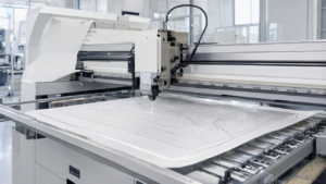
Precision and efficiency in cleaning and plating processes, long-standing hurdles in Panel-Level Packaging (PLP) and manufacturing, have been significantly advanced with the introduction of the Ultra C vac-p cleaning system and Ultra ECP ap-p plating system. Ultra C vac-p effectively removes flux residues prior to underfill, critically eliminating detrimental voids in fine bump pitches below 40µm and large chip sizes. Concurrently, the Ultra ECP ap-p plating system accommodates diverse plating applications such as pillars, bumps, and redistribution layers (RDLs), achieving superior uniformity and robust adhesion to glass panels through its unique multi-anode system and horizontal panel alignment. These innovations are accelerating the shift from circular wafers to large rectangular panels, maximizing package count per substrate area, and dramatically improving throughput, yield, and manufacturing costs.
Technical / Clinical Details
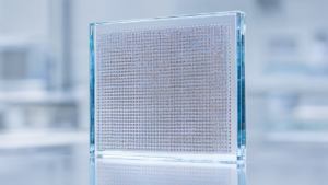
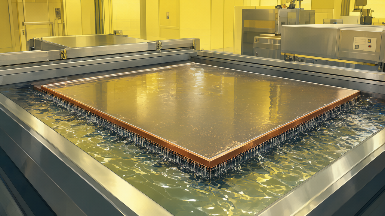
The Ultra C vac-p system leverages a vacuum-based precision cleaning process to reliably remove minute flux residues and other contaminants before underfilling. This is particularly crucial for preventing shorts or voids between fine-pitch bumps in chiplet, 2.5D, and 3D structures. Its efficacy is pronounced for bump pitches below 40µm and large chip sizes, substantially enhancing connection reliability. Meanwhile, the Ultra ECP ap-p plating system employs a unique multi-anode configuration and horizontal panel alignment during its electroplating process. The multi-anode system precisely controls the electric field distribution, ensuring exceptionally high uniformity of the plated film thickness across the entire panel. The horizontal panel arrangement optimizes plating solution flow, mitigating the risk of air bubble entrapment and particle adhesion. This system supports various advanced packaging plating processes, including pillar, micro-bump, and RDL formation, and demonstrates excellent adhesion, especially to novel substrate materials like glass panels. These technologies enable the manufacturing of high-quality, reliable packages in PLP with increased throughput and reduced costs.
Background & Context
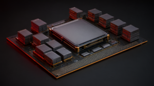
As semiconductor packaging technologies confront the physical limits of Moore’s Law, they have become a primary driver for enhancing system performance and reducing costs. The escalating demand for high-performance applications such as AI, HPC, and mobile devices necessitates denser, smaller, and more power-efficient packaging solutions. Panel-Level Packaging (PLP) offers significant advantages over traditional circular wafer-based packaging by utilizing large, rectangular panels, which improves material utilization efficiency and substantially reduces manufacturing costs. However, the adoption of PLP has been met with technical challenges, including achieving uniform cleaning across large substrates, precise plating, and compatibility with new materials (e.g., glass substrates). Advanced process solutions like Ultra C vac-p and Ultra ECP ap-p are indispensable for overcoming these hurdles and enabling the widespread adoption of PLP.
Strategic Significance & Outlook
The emergence of innovative technologies such as Ultra C vac-p and Ultra ECP ap-p significantly increases the likelihood of Panel-Level Packaging becoming a standard for next-generation semiconductor manufacturing. PLP’s efficiency and cost advantages will accelerate the proliferation of advanced packaging technologies like chiplets, 2.5D/3D integration, and Fan-Out Panel-Level Packaging (FOPLP). This is expected to reduce manufacturing costs for high-performance chips such as AI accelerators and HBM, promoting their wider application. Furthermore, the capability to accommodate new materials like glass substrates lays a crucial foundation for future packaging technologies demanding ultra-fine wiring and high-speed signal transmission. These advancements will play a vital role in enhancing manufacturing efficiency and competitiveness across the entire semiconductor industry supply chain.
Get our weekly technology intelligence — free
Receive an infographic that lets you judge at a glance whether each field’s analysis report is worth reading.
Subscribe Free — Weekly Tech Intelligence
By subscribing, you’ll receive Troy-Technical’s weekly technology intelligence newsletter.
- Your email and selected fields are used only to deliver the newsletter.
- We never share your information with third parties.
- You can unsubscribe anytime via the link in each email.
See our Privacy Policy for details.
Takes about a minute · Unsubscribe anytime