Key Findings
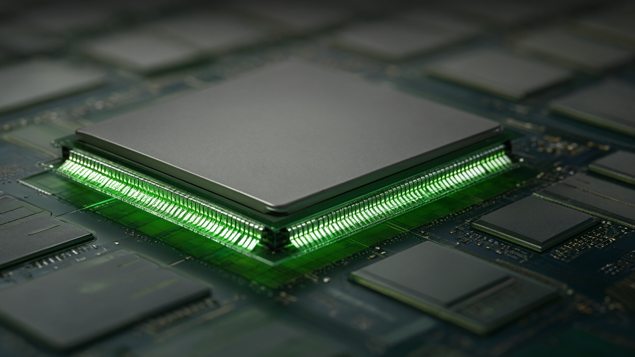
Micron Technology has unveiled a strategic shift for its custom HBM product, “NVHBM,” developed specifically for NVIDIA, announcing that it will utilize externally sourced base dies. According to NVIDIA, NVHBM integrates a customized physical layer (PHY), achieving a remarkable reduction of up to 67% in package area required for the I/O PHY. This innovation is projected to boost memory bandwidth by up to 30% and decrease HBM power consumption by 15% compared to standard HBM4E, positioning Micron to enhance HBM product profitability and reinforce its competitiveness in the high-performance AI chip market through this outsourced base die approach.
Technical / Clinical Details
The core innovation of NVHBM lies in its customized physical layer (PHY) integrated into the base die. This PHY circuit, optimized for NVIDIA’s specific AI accelerator designs, efficiently handles I/O signal transmission and reception. Such optimization dramatically reduces the I/O PHY area traditionally required in HBM packaging, leading to an impressive up to 67% reduction in overall package area. This reduction directly translates to lower manufacturing costs and increased packaging density. The enhanced efficiency of the I/O PHY also improves signal integrity, leading to higher data transfer rates. Consequently, NVHBM can achieve up to a 30% increase in memory bandwidth compared to standard HBM4E, directly contributing to superior data processing capabilities for AI workloads. Furthermore, the optimized power efficiency, resulting in a 15% reduction in HBM power consumption, holds significant implications for reducing data center operating costs and minimizing environmental impact.
Background & Context
The burgeoning AI semiconductor market has fueled an explosive demand for high-performance HBM. Leading AI chip manufacturers, particularly NVIDIA, require HBM with exceptionally high bandwidth, low power consumption, and compact package sizes to maximize GPU performance. For memory manufacturers, HBM production is complex and costly, making profitability a persistent challenge. Micron’s strategy of utilizing externally sourced base dies aims to concentrate its internal resources on memory stack manufacturing while mitigating the manufacturing costs and development risks associated with base dies. This approach allows Micron to supply custom HBM that meets NVIDIA’s stringent demands, optimizing cost-efficiency and time-to-market, thereby maintaining and strengthening its competitive edge in the rapidly growing AI market. This trend signifies a shift from vertical integration to horizontal specialization within the semiconductor supply chain, particularly highlighting the increasing importance of advanced packaging and custom solutions.
Strategic Significance & Outlook
Micron’s NVHBM strategy is poised to solidify its position in the AI semiconductor market. Collaborating with external foundries for base die procurement enhances HBM production flexibility, enabling rapid adaptation to market demand fluctuations. The projected up to 30% bandwidth increase and 15% power reduction are crucial for boosting the performance of NVIDIA’s next-generation AI accelerators, essential for training and inference of large-scale AI models. In the future, the development of such custom HBM products and collaboration with external ecosystems could become a new business model within the memory industry, accelerating HBM evolution in the AI era. This advancement is expected to drive progress in AI technologies across various domains, including data centers, edge AI, and high-performance computing.
Source: https://www.thelec.net/news/articleView.html?idxno=14372
Get our weekly technology intelligence — free
Receive an infographic that lets you judge at a glance whether each field’s analysis report is worth reading.
Subscribe Free — Weekly Tech Intelligence
By subscribing, you’ll receive Troy-Technical’s weekly technology intelligence newsletter.
- Your email and selected fields are used only to deliver the newsletter.
- We never share your information with third parties.
- You can unsubscribe anytime via the link in each email.
See our Privacy Policy for details.
Takes about a minute · Unsubscribe anytime